
Introduction to PCB Trace
Definition and Importance of PCB Trace
Printed Circuit Board (PCB) traces are the lifelines of any electronic device. They form the network of copper wiring, insulation, and fuses that make up a PCB. These traces are the pathways that allow electricity to flow, connecting various components and enabling the device to function.
Why are PCB traces so important? They are the backbone of the electronic world. Without them, your smartphone wouldn’t be smart, your laptop wouldn’t compute, and your gaming console wouldn’t provide any fun. They are the unsung heroes, quietly doing their job, ensuring that your devices work seamlessly.
Common Misconceptions about PCB Trace
Despite their importance, PCB traces are often misunderstood. One common misconception is that all traces are the same. However, the truth is that each trace is unique and carefully designed to meet the specific requirements of the device it’s part of.
Another misconception is that traces are simple and easy to design. In reality, PCB trace design is a complex process that requires a deep understanding of electrical engineering principles, materials, and manufacturing techniques.
So, what’s the takeaway here? PCB traces might seem like just tiny lines on a board, but they are much more than that. They are a testament to the marvels of modern engineering and the cornerstone of our digital age.
The Role of PCB Trace in Circuit Board Design
The Impact of PCB Trace on Electronic Devices
PCB traces are more than just conduits for electrical current; they are the heart of every electronic device. Each trace is meticulously designed and placed to ensure optimal performance. The layout of these traces can significantly influence the efficiency, reliability, and overall functionality of the device.
For instance, consider a smartphone. A well-designed trace in a smartphone can reduce electromagnetic interference, improve signal integrity, and enhance the device’s power efficiency. This could mean clearer phone calls, faster data processing, and longer battery life. Conversely, a poorly designed trace can lead to signal degradation, power loss, and even device failure, resulting in dropped calls, slow performance, and frequent charging.
The Importance of Correctly Detecting and Calculating PCB Trace
Detecting and calculating PCB trace is not just a task; it’s an art. It requires a deep understanding of the device’s requirements, the properties of the materials used, and the principles of electrical engineering.
Incorrect detection or calculation of PCB trace can lead to serious consequences, such as overheating, short circuits, and even device failure. For example, if the trace width is miscalculated in a high-power device, it could lead to overheating and potentially a fire. On the other hand, accurate detection and calculation can ensure that the device operates at its peak efficiency, extending its lifespan and improving its performance.
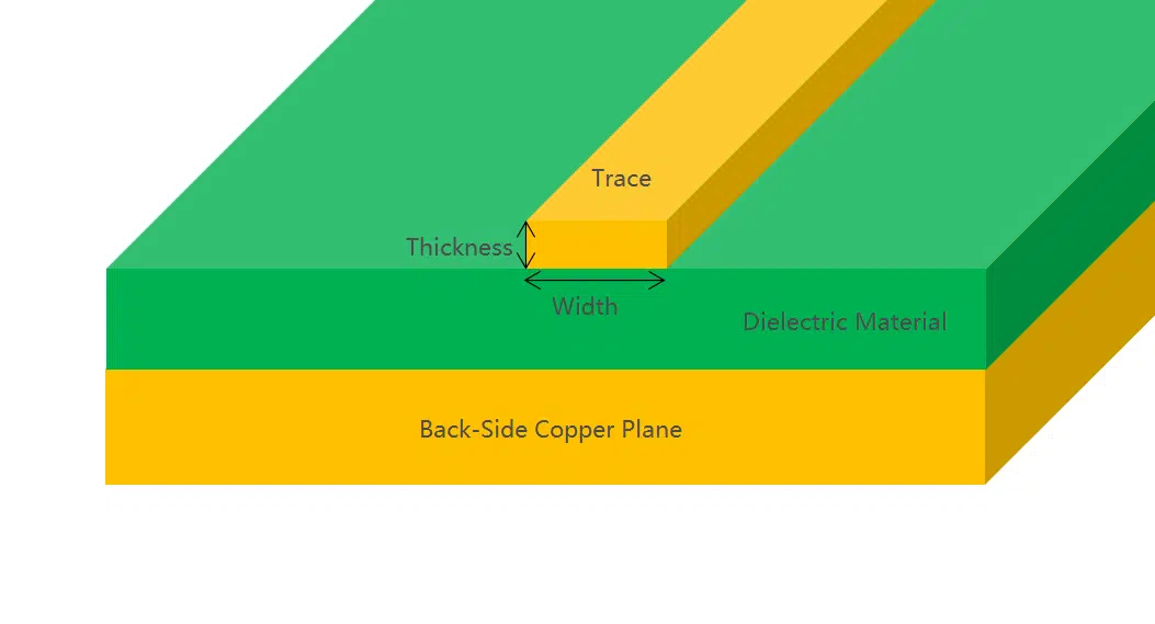
The Significance of PCB Trace Thickness in PCB Design
The Balance Maintained by PCB Trace Thickness
In the world of PCB design, trace thickness plays a pivotal role. It’s not just about the physical dimensions; the thickness of a PCB trace can significantly impact the performance and reliability of an electronic device.
The thickness of a trace determines its current-carrying capacity, or how much electrical current it can safely handle without overheating. This is crucial because an overheated trace can lead to device failure.
Moreover, the thickness of a trace can influence the device’s electromagnetic compatibility. A thicker trace can reduce electromagnetic interference, ensuring that the device operates smoothly without any disruptions.
Common Ranges of PCB Trace Thickness and Their Implications
PCB trace thickness varies depending on the specific requirements of the device. Common ranges include 0.008 inches to 0.240 inches. However, the choice of thickness is not arbitrary; it’s a careful decision made by the PCB designer based on several factors.
For instance, a high-power device might require thicker traces to handle larger currents. On the other hand, a compact device with limited space might require thinner traces.
It’s also worth noting that the thickness of a trace can affect its resistance and impedance, which in turn can impact signal integrity. Therefore, choosing the right trace thickness is a delicate balance between meeting the device’s electrical requirements and ensuring its physical compatibility.
| PCB Trace Thickness | Current Capacity | Electromagnetic Interference | Suitability for Compact Devices | Resistance and Impedance |
|---|---|---|---|---|
| Thicker | Higher | Lower | Less Suitable | Lower |
| Thinner | Lower | Higher | More Suitable | Higher |
PCB Trace Thickness and Signal Speed
In high-frequency PCB design, the thickness of a trace can have a significant impact on signal speed and quality. This is due to a phenomenon known as skin effect, where the signal tends to propagate along the surface (or “skin”) of the conductor.
As the frequency of the signal increases, the skin depth decreases, meaning the signal uses less of the conductor’s cross-sectional area. This effectively increases the resistance of the trace, which can lead to signal degradation.
Therefore, in high-frequency applications, PCB designers often use thicker traces or even consider using different materials to mitigate the skin effect and maintain signal integrity.
In conclusion, the thickness of a PCB trace is not just a number; it’s a critical factor that can make or break the performance of an electronic device. As such, it’s one of the many aspects that PCB designers need to consider and optimize when creating a PCB.
PCB Trace Width: An Essential Design Parameter
The Relationship Between Trace Width and Current Transfer
The width of a PCB trace is directly related to its current-carrying capacity. A wider trace can carry more current due to its larger cross-sectional area, which reduces resistance and allows more current to pass. This is particularly important in devices where large amounts of current need to be transferred, such as power amplifiers or motor controllers.
How to Calculate PCB Trace Width
| Trace Location | k Value | b Value | c Value |
|---|---|---|---|
| External Layer | 0.048 | 0.44 | 0.725 |
| Internal Layer | 0.024 | 0.44 | 0.725 |
Calculating the appropriate trace width for a PCB is a vital part of the design process. One commonly used method is the IPC-2221 formula. This formula considers factors such as the maximum current, trace thickness, and ambient temperature. Here’s a simplified version of the formula:
Trace Width (in mils) = (Current (in Amps) / (k * (Temperature Rise in °C)^b)) ^ (1/c)In this formula, k, b, and c are constants that depend on whether the trace is in the air (external layer) or in the board (internal layer). For external layers, k = 0.048, b = 0.44, and c = 0.725. For internal layers, k = 0.024, b = 0.44, and c = 0.725.
Let’s take an example. Suppose we have a PCB with an external trace carrying a current of 2 Amps, and we want to limit the temperature rise to 10°C. Plugging these values into the formula gives:
Trace Width = (2 / (0.048 * (10)^0.44)) ^ (1/0.725) = 66.7 milsThis means that for a 2 Amps current and a temperature rise of 10°C, the trace width should be approximately 66.7 mils.
Remember, this is a simplified version of the IPC-2221 formula, and actual PCB design may require more complex calculations and considerations. Always consult with a qualified PCB designer or engineer when designing a PCB.
Limitations and Alternatives to the IPC-2221 Formula
While the IPC-2221 formula is a useful tool, it’s important to be aware of its limitations. The formula assumes certain conditions that may not always hold true in real-world applications. For instance, it assumes a certain level of heat dissipation that might not be achievable in a compact device with limited airflow.
Moreover, the IPC-2221 formula is just one of many methods for calculating PCB trace width. Other methods may take into account additional factors such as the frequency of the signal, the dielectric constant of the PCB material, and the desired impedance.
Practical Tips for Implementing PCB Trace Width
When designing a PCB, it’s crucial to balance the need for a wider trace (for higher current capacity) with the need to conserve space on the PCB. Here are a few tips:
- Start with the IPC-2221 formula (or another suitable method) to get a rough estimate of the required trace width.
- Consider the specific conditions of your device, such as the expected operating temperature and the available space for traces.
- Keep in mind that wider traces can help reduce electromagnetic interference, which can be particularly beneficial in high-frequency applications.
- Always verify your design with a qualified PCB designer or engineer before proceeding to fabrication.
Remember, this is a simplified version of the IPC-2221 formula, and actual PCB design may require more complex calculations and considerations. If you’re unsure or need professional assistance, don’t hesitate to reach out to us at Rowsum. Our team of experienced PCB designers and engineers are always ready to help you optimize your PCB design for maximum performance and reliability.
The Complexity of Calculating Trace Width
| Factor | Description |
|---|---|
| Current Capacity | The maximum current that the trace will need to carry. |
| Signal Integrity | The quality of the signal that the trace carries. |
| PCB Material | The properties of the PCB material, such as its thermal conductivity and dielectric constant. |
| Environmental Conditions | The expected operating conditions of the device, such as the ambient temperature and humidity. |
Factors Influencing Trace Width Calculation
Calculating the appropriate trace width for a PCB is not a straightforward task. It involves a complex interplay of several factors, each of which can significantly impact the performance and reliability of the final product. Here are some of the key factors that need to be considered:
- Current Capacity: The trace width must be sufficient to safely carry the maximum current that the device will require. This is crucial to prevent overheating and potential device failure.
- Signal Integrity: The trace width can affect the quality of the signal that it carries. A trace that is too narrow can lead to increased resistance and potential signal degradation, while a trace that is too wide can increase the risk of cross-talk and other forms of electromagnetic interference.
- PCB Material: The properties of the PCB material, such as its thermal conductivity and dielectric constant, can influence the optimal trace width. Different materials may require different trace widths to achieve the same performance.
- Environmental Conditions: The expected operating conditions of the device, such as the ambient temperature and humidity, can also affect the trace width calculation. For example, a device that is expected to operate in a high-temperature environment may require wider traces to ensure adequate heat dissipation.
The Challenge of Balancing Multiple Factors
Balancing these factors is a complex task that requires a deep understanding of electrical engineering principles and practical experience in PCB design. It’s not just about finding a trace width that meets the current capacity requirements; it’s about optimizing the trace width to achieve the best possible performance under the specific conditions that the device will face.
This is where the expertise of a professional PCB designer or engineer can be invaluable. They can help navigate the complexities of trace width calculation and ensure that the final design is robust, reliable, and efficient. If you need assistance with your PCB design, don’t hesitate to reach out to us at Rowsum. Our team of experienced professionals is always ready to help.
The Importance of PCB Trace Current in PCB Fabrication
Understanding PCB Trace Current
PCB trace current, the flow of electric charge along the trace, is a fundamental aspect of PCB design and fabrication. The amount of current a trace can safely carry, its current capacity, is determined by factors such as the trace’s width, thickness, and the material from which it’s made.
The Role of PCB Trace Current in Device Performance
The current capacity of a PCB trace directly impacts the performance of the electronic device. If a trace can’t carry the required current, the device may not function correctly, or the trace could overheat, potentially leading to device failure.
Practical Tips for Managing PCB Trace Current
Designing PCB traces to handle the appropriate current is a delicate balance. Here are some practical tips:
- Optimize Trace Dimensions: Use the IPC-2221 formula or similar methods to calculate the optimal trace width for your current requirements. Remember that thicker and wider traces can carry more current. For example, if you’re designing a PCB for a high-power device, you might need to use wider traces than you would for a low-power device.
- Choose the Right Materials: Different PCB materials have different resistances and thermal properties. Choose a material that can handle your device’s current and heat dissipation needs. For instance, a material with a high thermal conductivity, such as copper, can help dissipate heat more effectively and allow for higher current capacities.
- Consider Thermal Management: For high-current applications, consider using heat sinks or other thermal management solutions to help dissipate heat and prevent overheating. This could involve designing your PCB layout to include space for heat sinks, or using materials with better thermal properties.
- Verify Your Design: Always double-check your design and calculations with a qualified PCB designer or engineer. This can help you avoid costly mistakes and ensure that your PCB will function as intended. For example, you might want to use simulation software to verify that your trace widths are sufficient for your current requirements.
In conclusion, managing PCB trace current is a vital aspect of PCB design and fabrication. It impacts not only the performance and reliability of the electronic device but also the efficiency and cost-effectiveness of the fabrication process.
Conclusion: The Impact of PCB Trace on PCB Design and Fabrication
Understanding the intricacies of PCB trace design, including trace width, current capacity, and the complexities of calculating these parameters, is crucial for creating efficient and reliable electronic devices. The trace width and current capacity directly influence the performance of the device, the efficiency of the fabrication process, and the overall cost-effectiveness of the product.
Balancing these factors is a complex task that requires a deep understanding of electrical engineering principles and practical experience in PCB design. It’s not just about finding a trace width that meets the current capacity requirements; it’s about optimizing the trace width to achieve the best possible performance under the specific conditions that the device will face.
At Rowsum, we understand the complexities of PCB design and fabrication. Our team of experienced professionals is always ready to assist you in optimizing your PCB design for maximum performance and reliability. We are committed to providing high-quality PCB products to our clients, prioritizing quality, reliability, and excellent customer service.
Frequently Asked Questions about PCB Trace
Q1: What is the IPC-2221 formula?
A1: The IPC-2221 formula is a commonly used method for calculating the appropriate trace width for a PCB. It takes into account factors such as the maximum current, trace thickness, and ambient temperature.
Q2: How does trace width affect the performance of a PCB?
A2: The width of a PCB trace directly affects its current-carrying capacity. A wider trace can carry more current, which is particularly important in devices where large amounts of current need to be transferred.
Q3: What factors should be considered when calculating trace width?
A3: Several factors should be considered when calculating trace width, including the maximum current the trace will need to carry, the thickness of the trace, the material from which the PCB is made, and the expected operating conditions of the device.
Q4: How does PCB trace current affect the fabrication process?
A4: The current capacity of a trace influences the fabrication process. Traces designed to carry higher currents require more copper, which can affect the etching process used to create the traces on the PCB.
Q5: Where can I get help with my PCB design?
A5: At Rowsum, our team of experienced professionals is always ready to assist you with your PCB design needs. We are committed to providing high-quality PCB products and excellent customer service.