Introduction
Have you ever wondered how the intricate circuits in your electronic devices are made? How do the various components communicate with each other across different layers of a Printed Circuit Board (PCB)? What if I told you that a tiny hole, often overlooked, plays a crucial role in this complex dance of signals? This tiny hole, known as a ‘via’, is a fundamental part of PCB design and manufacturing. But there’s more to it than just drilling a hole. One of the key processes involved is something called ‘tenting’.
But what exactly is tenting via, and why is it so important in PCB fabrication?
Tenting via is a popular and mature process in PCB fabrication. It involves covering the annular ring and via hole with a protective layer, often a solder mask. This simple yet effective process is crucial for preventing exposure to elements, reducing accidental shorting, and ensuring the overall reliability of the PCB. In the world of PCB manufacturing, tenting via is not just a process; it’s a strategy for success.
In the following sections, we’ll delve deeper into the world of tenting via, exploring its advantages, alternatives, and its importance in the PCB manufacturing industry. Whether you’re a seasoned PCB designer, a procurement manager who values efficiency and quality, or simply an electronics enthusiast, this article will provide you with valuable insights into the fascinating world of PCB manufacturing.
So, are you ready to uncover the secrets of tenting via? Let’s dive in!
What is a Via in PCB Manufacturing?
Have you ever looked closely at a Printed Circuit Board (PCB)? If you have, you might have noticed a series of tiny holes scattered across the board. These are not random or accidental; they are an integral part of the PCB design and are known as ‘vias’.
But what exactly is a via?
In the simplest terms, a via is a conduit that allows electrical signals to travel from one layer of the PCB to another. It’s like a tunnel that connects different layers of a city, allowing traffic to flow smoothly from one level to another.
Vias are typically made by drilling holes into the PCB and then plating them with a conductive material, usually copper. This is because copper is an excellent conductor of electricity, making it ideal for transmitting signals across the PCB.
But why are vias so important in PCB manufacturing?
Well, as electronic devices become more complex and compact, the need for multi-layer PCBs has increased. These multi-layer PCBs require a way for signals to move between layers, and that’s where vias come in. They provide the necessary interconnections that make the functioning of these complex PCBs possible.
In essence, vias are the unsung heroes of PCB manufacturing, playing a crucial role in the functionality and performance of electronic devices. But as with any hero, they need protection to perform their best. And that’s where tenting via comes into play. But before we delve into that, let’s take a moment to understand the different types of vias used in PCB manufacturing.
Tenting Via: A Closer Look
So, what exactly does it mean to ‘tent’ a via?
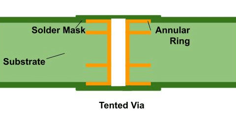
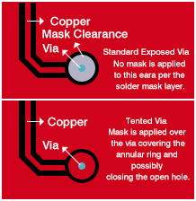
In the world of PCB manufacturing, tenting a via refers to the process of covering the via, specifically the annular ring and the via hole, with a protective layer. This layer is often a solder mask, a material commonly used in PCB manufacturing to protect the copper traces from oxidation and corrosion.
But why is it called ‘tenting’?
The term ‘tenting’ comes from the visual appearance of the process. When the solder mask is applied over the via, it forms a ‘tent-like’ structure, covering and protecting the via from external elements.
How is tenting via done?
The process of tenting via is relatively straightforward. After the vias are drilled and plated, a layer of solder mask is applied over the entire PCB. This solder mask naturally covers the vias, forming a ‘tent’ over them. No special steps are taken to ensure the hole opening remains closed. Sometimes, the hole remains covered, but there is no guarantee, especially with larger diameter vias.
What makes tenting via so special?
Tenting via has several advantages that make it a popular choice in PCB manufacturing. It provides protection to the vias, prevents accidental shorting or contact with the circuit, and is particularly useful in areas where Surface Mount Technology (SMT) pads are placed close to vias.
In short, tenting via is a simple yet effective strategy in PCB manufacturing, providing a layer of protection that enhances the reliability and longevity of the PCB. But as with any strategy, it’s not the only one. In the next section, we’ll explore some alternatives to tenting via and see how they compare. So, let’s continue our journey into the fascinating world of PCB manufacturing!
Alternatives to Tenting Via
| Method | Cost | Effectiveness in Preventing Shorting | Suitability for Different PCB Designs |
|---|---|---|---|
| Tenting Via | Low | High | Suitable for most designs |
| Plugging | Medium | High | Suitable for designs requiring a flat surface |
| Capping | High | High | Suitable for designs requiring additional protection |
While tenting via is a popular and effective method in PCB manufacturing, it’s not the only strategy for protecting vias. There are several other techniques that PCB manufacturers use, each with its own set of advantages and considerations. Let’s take a closer look at some of these alternatives.
Plugging Vias
One alternative to tenting is plugging vias. This process involves filling the via hole with a non-conductive material, often an epoxy resin. Plugging vias provides a higher level of protection than tenting, as it completely seals the via hole, preventing any exposure to external elements. However, this method is more expensive and time-consuming than tenting, making it less suitable for cost-sensitive or high-volume projects.
Capping Vias
Another alternative is capping vias. In this process, the via hole is filled with a conductive or non-conductive material, and then a cap is placed over the top. This method provides a high level of protection and can also improve the surface planarity of the PCB, making it more suitable for certain assembly processes. However, like plugging, capping vias is more expensive and time-consuming than tenting.
Masking Vias
Masking is another method used to protect vias. This process is similar to tenting, but instead of just covering the annular ring and via hole, the entire via is covered with a solder mask. This provides a higher level of protection than tenting, but it can also increase the complexity of the PCB assembly process, as it requires more precise control over the solder mask application.
In conclusion, while tenting via is a popular and cost-effective method for protecting vias in PCB manufacturing, it’s not the only option. Depending on the specific requirements of the PCB design and the resources available, PCB manufacturers may choose to use plugging, capping, or masking vias instead. Each method has its own set of advantages and considerations, and the best choice often depends on the specific circumstances of the project.
The Advantages of Tenting Via
| Advantage | Explanation |
|---|---|
| Prevents Accidental Shorting | Tenting via covers the via with a protective material, preventing solder from accidentally flowing into the via during assembly. |
| Protects from Environmental Exposure | The protective cover shields the via from environmental factors like moisture and dust. |
| Enables High-Density PCB Designs | Tenting via allows for closer placement of vias without increasing the risk of shorting, enabling high-density, space-efficient PCB designs. |
| Cost-Effective | Tenting via uses standard materials and processes, contributing to cost savings in PCB production. |
Tenting via is a widely adopted method in PCB manufacturing, and for good reason. It offers a range of benefits that contribute to the efficiency, reliability, and overall success of the PCB fabrication process. Let’s explore some of these advantages in more detail.
Protection of PCB Layers
One of the primary advantages of tenting via is the protection it provides to the PCB layers. By covering the via with a solder mask, it shields the copper traces from exposure to external elements, preventing oxidation and corrosion. This is crucial for maintaining the integrity and longevity of the PCB.
Reduction of Conductive Component Exposure
Tenting via also reduces the number of conductive components exposed to external elements. This is particularly important in complex PCB designs where vias are placed close to other components. By tenting the via, the risk of accidental shorting or contact with the circuit is significantly reduced.
Cost-Effectiveness
Tenting via is a cost-effective method for protecting vias in PCB manufacturing. The process involves using a solder mask, which is a standard material in PCB fabrication, and does not require any additional steps or materials. This makes it a practical choice for PCB manufacturers, especially for high-volume projects.
Improved PCB Assembly Process
Tenting via can also contribute to a smoother PCB assembly process. By covering the vias, it reduces the likelihood of solder bridging during the assembly process. This can lead to fewer assembly issues and higher yield rates, making the overall manufacturing process more efficient.
In essence, tenting via offers a simple yet effective solution for protecting vias in PCB manufacturing. It combines protection, efficiency, and cost-effectiveness, making it a preferred choice for many PCB manufacturers. But as with any method, it’s important to consider the specific requirements of the
Detailed Analysis and Case Studies
To provide a more comprehensive understanding of the advantages of tenting via, let’s delve deeper into some specific scenarios and expert insights.
- Case Study: Protection Against Environmental Factors
In a high-humidity environment, unprotected vias can become a pathway for moisture ingress, leading to potential damage and failure of the PCB. Tenting vias can effectively prevent this issue by sealing the via hole, providing a barrier against moisture and other environmental factors. This is particularly beneficial in applications such as outdoor electronics, where PCBs are exposed to varying weather conditions.
- Expert Insight: Via Filling and Via-in-Pad Applications
According to a detailed article by Eurocircuits, the resin used for tenting vias is suitable for Via-in-Pad applications. Via-in-Pad is a design technique in which vias are placed directly under component pads. This technique is often used in high-density designs where space is limited. Tenting these vias can prevent solder from wicking into the via during assembly, ensuring a reliable solder joint.
- Case Study: Cost-Effectiveness in High-Volume Production
For high-volume PCB production, cost-effectiveness is a crucial factor. Tenting vias is a cost-effective method as it uses standard materials (solder mask) and does not require additional process steps. This makes it a practical choice for large-scale PCB manufacturing, contributing to overall cost savings.
- Expert Insight: Improved PCB Assembly Process
Tenting vias can contribute to a smoother PCB assembly process by reducing the likelihood of solder bridging during the assembly process. Solder bridging is a common issue in PCB assembly where solder forms unintended connections between conductive areas. By tenting the vias, the risk of solder bridging is significantly reduced, leading to fewer assembly issues and higher yield rates.
In conclusion, tenting via offers a multitude of advantages from various perspectives, including environmental protection, application in high-density designs, cost-effectiveness, and improved assembly process. These benefits make it a preferred choice for many PCB manufacturers and designers. However, it’s important to consider the specific requirements of the PCB design and the resources available when choosing the best method for via protection.
The Importance of Tenting Via in PCB Manufacturing
While we’ve discussed the advantages of tenting via, it’s also crucial to understand its broader significance in the PCB manufacturing industry and the impact on the end products – the electronic devices we use every day.
Ensuring Reliability of Electronic Devices
Tenting via plays a vital role in ensuring the reliability of electronic devices. By protecting the vias from environmental exposure and accidental shorting, tenting via contributes to the longevity and performance of the PCB, and by extension, the electronic device itself. This is particularly important in devices where reliability and durability are paramount, such as medical devices, aerospace electronics, and industrial machinery.
Enabling Advanced PCB Designs
As electronic devices become smaller and more complex, PCB designs must follow suit. Tenting via enables advanced PCB designs by allowing for higher via densities without increasing the risk of shorting or solder bridging. This is crucial in modern electronics, where space is often at a premium.
Contributing to Cost-Effective Manufacturing
From a manufacturing perspective, tenting via is a cost-effective method for via protection. It uses standard materials and processes, which can contribute to overall cost savings in PCB production. This can translate to more competitively priced electronic products, benefiting both manufacturers and consumers.
Meeting Industry Standards
Tenting via also helps PCB manufacturers meet industry standards for PCB design and manufacturing. For instance, the IPC-4761 standard for via protection recommends tenting as one of the acceptable methods for via protection.
Case Study: Farm Monitoring Equipment
Let’s consider a real-life example from one of our clients, a leading company in the agricultural technology sector. They specialize in developing advanced farm monitoring equipment, devices that help farmers monitor various parameters like soil moisture, temperature, and crop health. These devices play a crucial role in modern farming, enabling farmers to make informed decisions and optimize their crop yield.
One of their flagship products is a compact, handheld monitoring device. This device is packed with a multitude of sensors and communication modules, all integrated into a multi-layer PCB. Given the high density of components and the outdoor usage of the device, the PCB design and manufacturing process had to address several challenges.
The vias on the PCB were placed extremely close to each other and to other components due to space constraints. This high-density environment increased the risk of accidental shorting or solder bridging during assembly. Moreover, as the device was to be used in outdoor farming conditions, the PCB had to withstand various environmental factors like moisture, dust, and temperature fluctuations.
To address these challenges, our team decided to implement tenting via in the PCB manufacturing process. By covering the vias, we were able to prevent solder from accidentally flowing into the via during assembly, significantly reducing the risk of shorting. The tenting also provided an additional layer of protection against environmental factors, enhancing the durability and lifespan of the device.
The result was a robust, reliable farm monitoring device that performed excellently in field conditions. The client was extremely satisfied with the product, and it has since become one of their best-selling items.
In conclusion, the importance of tenting via in PCB manufacturing is evident in real-world applications. It plays a crucial role in ensuring the reliability and performance of electronic devices, enabling advanced PCB designs, and meeting industry standards. By understanding its significance, we can appreciate the intricate processes that go into creating the electronic devices we rely on every day.
Rowsum’s Approach to Tenting Via in PCB Manufacturing
| Key Aspect | Description |
|---|---|
| Quality and Reliability | Rowsum uses tenting via to enhance the longevity and performance of PCBs. |
| Advanced PCB Designs | Rowsum leverages tenting via to create high-density, space-efficient PCB designs. |
| Cost-Effective Solutions | Rowsum integrates the tenting via process into the standard PCB manufacturing process to provide cost-effective solutions. |
| Personalized Service | Rowsum provides a dedicated project manager to follow up on each project 1V1. |
When it comes to tenting via in PCB manufacturing, we at Rowsum have a pretty straightforward approach. We believe in doing things right, and here’s how we make it happen:
- Quality and Reliability
We’re sticklers for quality. Each via on our PCBs is carefully tented, a small step that makes a big difference. It’s like putting a protective shield on each via, keeping them safe from environmental exposure and reducing the risk of accidental shorting. It’s these little details that help our PCBs stand the test of time and keep performing at their best.
- Advanced PCB Designs
Our team is pretty good at solving puzzles. Fitting more components on a PCB is a bit like a puzzle, and tenting via is one of the tools we use. It allows us to place vias close to other components without increasing the risk of shorting, enabling us to create high-density, space-efficient PCB designs. It’s all about making the most of the space we have.
- Cost-Effective Solutions
We’re all about providing value. By integrating the tenting via process into our standard PCB manufacturing process, we’re able to keep costs down without compromising on quality. It’s like getting a premium feature without the premium price tag.
- Personalized Service
We believe in the personal touch. When you work with us, you’ll have a dedicated project manager to follow up on your project 1V1. It’s like having a friend in the business who’s always ready to help out with any technical issues.
So, if you’re looking for a PCB solution that’s reliable, efficient, and cost-effective, why not give us a try? Feel free to drop us a line at [email protected] or check us out at www.rowsum.com. We’re always here to help.
Conclusion
Tenting via is a crucial aspect of PCB manufacturing, playing a significant role in ensuring the reliability and performance of electronic devices. It enables advanced PCB designs, contributes to cost-effective manufacturing, and helps meet industry standards. Whether you’re a PCB designer, a manufacturer, or simply an enthusiast, understanding the importance of tenting via can provide valuable insights into the intricate processes that go into creating the electronic devices we rely on every day.
At Rowsum, we’re committed to delivering high-quality, reliable, and cost-effective PCB solutions. Our approach to tenting via reflects this commitment. If you’re looking for a PCB solution, feel free to reach out to us. We’re always ready to assist you.
Frequently Asked Questions
Q1: What is tenting via in PCB manufacturing?
A: Tenting via is a process in PCB manufacturing where the vias (holes that allow electrical connection between different layers of a PCB) are covered with a protective material, usually solder mask, to prevent solder from accidentally flowing into the via during assembly.
Q2: Why is tenting via important in PCB manufacturing?
A: Tenting via is important as it helps prevent accidental shorting during assembly, protects the vias from environmental exposure, enables advanced, high-density PCB designs, and contributes to cost-effective manufacturing.
Q3: How does Rowsum approach tenting via in PCB manufacturing?
A: At Rowsum, we prioritize quality and reliability, using tenting via to enhance the longevity and performance of our PCBs. We also provide personalized service, with a dedicated project manager to follow up on each project 1V1.
Q4: What are the alternatives to tenting via?
A: Alternatives to tenting via include plugging, where the via is filled with non-conductive or conductive material, and capping, where a cap of solder mask or metal is placed over the via.
Q5: How does tenting via contribute to cost-effective PCB manufacturing?
A: Tenting via is a cost-effective method for via protection as it uses standard materials and processes, which can contribute to overall cost savings in PCB production.
Get Access Now: www.rowsum.com