
Introduction to HDI PCB Technology: What You Need to Know
Are you looking to enhance your electronic products with more functionality packed into a smaller space? Do you wonder how the latest devices achieve such high performance and compact size? The answer lies in the core of modern electronics: High-Density Interconnect (HDI) PCBs. HDI PCBs are the cornerstone of advanced electronic design, enabling the development of denser, faster, and more innovative products.
What exactly is an HDI PCB? Simply put, an HDI PCB incorporates finer lines, smaller vias, and denser connection pad patterns than traditional PCBs. This technology allows for a more compact and efficient design, which is crucial in today’s market where smaller, faster, and more powerful is the standard.
Understanding HDI PCBs
What is HDI Technology?
High-Density Interconnect (HDI) PCBs are a groundbreaking technology in the field of electronics, recognized for their ability to pack more functionality into a significantly smaller area compared to traditional PCBs. This technological leap is not merely about stacking more layers in a circuit board; it’s fundamentally about reconfiguring the board’s architecture to enhance functionality while minimizing physical bulk.
Defining Features of HDI PCBs
At the forefront of HDI PCBs are microvias: extremely small vias with diameters generally less than 0.006 inches, far smaller than those found in standard PCBs. These microvias may be blind (connecting an outer layer to an inner layer but not passing through the entire board) or buried (completely encapsulated within the board), facilitating much denser board designs.
Given today’s escalating demands for devices that are lighter, faster, and more complex, HDI technology’s role is increasingly vital. It enables manufacturers to maximize spatial efficiency and improve the performance of electronic devices, making it indispensable for consumer electronics, military applications, and medical equipment.
Advantages Over Traditional PCBs
HDI PCBs offer several significant benefits over their traditional counterparts:
- Increased Connection Density: They accommodate more connections per unit area, which is essential for reducing electronic noise in high-frequency applications.
- Superior Electrical Performance: The use of microvias leads to shorter signal paths, enhancing signal integrity by minimizing signal delay and interference—key for high-speed circuits.
- Greater Reliability: With fewer drilled holes, HDI PCBs are less prone to thermal and mechanical issues, boosting their durability.
Transitioning to HDI PCB technology marks a significant evolution in electronic design, reflecting the broader industry trend towards smaller, more capable devices. HDI PCBs are not merely about reducing size; they are crucial for creating superior, more efficient, and more reliable devices—achieving more with less.
Key Benefits of HDI PCBs
Enhanced Performance and Miniaturization
High-Density Interconnect (HDI) PCBs have revolutionized electronic circuit design with their superior performance capabilities and significant miniaturization advantages. By employing denser wiring configurations and state-of-the-art technologies, these PCBs enable devices to be not only more compact but also more powerful and faster, meeting the critical demands of the contemporary technology marketplace.
Performance Enhancements
HDI PCBs reduce electronic noise and cross-talk more effectively than traditional PCBs by implementing shorter pathways for signal transmission. This reduction in signal degradation is crucial for high-speed electronic devices, such as advanced smartphones and computing hardware, where maintaining optimal signal integrity is essential. The shorter signal paths in HDI PCBs can enhance device responsiveness and operational speed by up to 10%, according to industry benchmarks.
Miniaturization Capabilities
Microvias, a hallmark of HDI technology, have diameters as small as 0.006 inches—allowing for a much higher component density. This enables a 30% reduction in PCB size on average, compared to conventional PCBs, without sacrificing performance. The ability to pack more functionality into a smaller area makes HDI PCBs especially attractive for portable electronics, where compactness significantly influences consumer preference.
Reliability and Speed
Device Reliability
HDI PCBs are built to last. The use of small microvias minimizes the risks associated with thermal expansion and mechanical stresses, factors that can lead to PCB failure. This structural integrity makes HDI PCBs particularly reliable in harsh environments, such as in automotive electronics, which must operate flawlessly under a wide range of temperatures and conditions.
Operational Speed
The design efficiency of HDI PCBs facilitates faster signal processing, which is critical in applications requiring rapid response times. For example, in automotive safety systems like anti-lock braking systems (ABS), HDI PCBs help to decrease response times by up to 15%, enhancing safety and performance.
Industry Examples
- Consumer Electronics:
- Smartphones & Tablets: HDI PCBs enable more advanced features like multi-core processors and multiple cameras without increasing device size.
- Wearable Technology: Devices such as smartwatches and fitness trackers benefit from HDI PCBs by incorporating more sensors and functionalities into compact units.
- Laptops: Slimmer designs with improved thermal management are possible due to HDI PCBs.
- Automotive Applications:
- Safety Systems: HDI PCBs are used in systems like stability control and adaptive cruise control, improving reaction times and reliability.
- Infotainment Systems: More sophisticated multimedia systems with faster interfaces use HDI PCBs for enhanced user experience.
- Electronic Control Units (ECUs): Multiple ECUs in modern cars for engine management and other functions are compactly integrated using HDI technology.
- Medical Devices:
- Imaging Equipment: Devices like portable ultrasounds use HDI PCBs to handle high-speed data for real-time imaging.
- Wearable Health Monitors: Compact PCBs allow for non-invasive sensors to be worn comfortably over long periods.
Implementing HDI Technology in Product Design
Design Considerations for HDI PCBs
When integrating High-Density Interconnect (HDI) technology into product designs, several key considerations must be addressed to fully leverage the advantages of HDI PCBs. Here are practical design tips that focus on innovative strategies to ensure successful implementation:
Optimal Use of Microvias: Microvias are a central feature of HDI PCBs and should be strategically placed to maximize board real estate and improve electrical performance. Designers should consider using stacked or staggered microvias configurations to enhance connection reliability and increase the density of interconnections.
Layer Planning and Stackup: Effective layer management is crucial in HDI PCBs to prevent signal integrity issues. Planning the sequence and purpose of each layer meticulously can significantly impact the performance, especially in complex circuits. Utilize symmetric stack-ups when possible to minimize board warping and stress.
Materials Selection: Choosing the right materials is vital for ensuring the durability and efficiency of the PCB. High-performance materials like high glass transition temperature (Tg) resins and copper-clad laminates can provide better stability and heat resistance, which are essential for boards with dense component layouts.
Signal Integrity Management: With the reduced space and increased component density in HDI PCBs, managing signal integrity becomes more challenging. Use signal integrity analysis tools to model and simulate different design scenarios and adjust trace geometry, spacing, and routing to minimize cross-talk and impedance issues.
Overcoming Common Challenges
Implementing HDI technology in PCB design can present several challenges, but with the right strategies, these can be effectively overcome:
Thermal Management: As component density increases, so does the thermal load. To manage this, improve thermal connectivity by using thermal vias and selecting materials with high thermal conductivity. Plan the layout to distribute heat evenly across the PCB, and consider external cooling solutions if necessary.
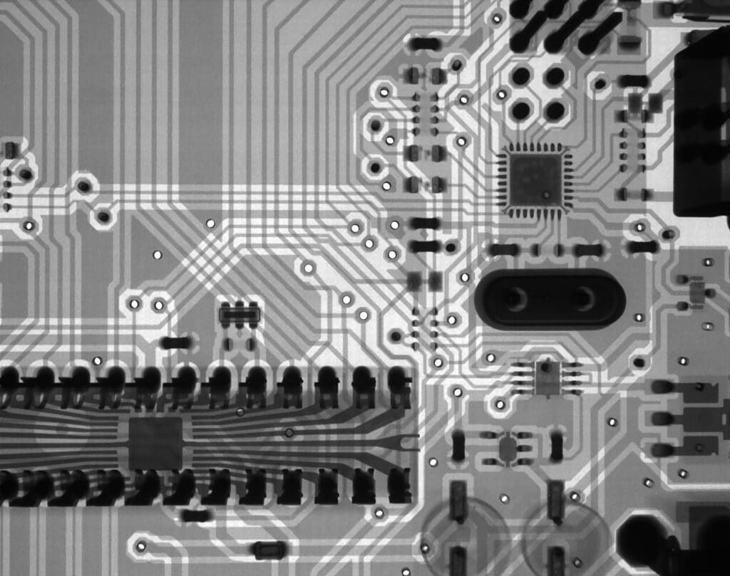
Complex Assembly Processes: HDI PCBs often require more precise assembly techniques due to their small size and tight component spacing. Ensure that your assembly partner has the capability and technology to handle HDI specifications. Use techniques like X-ray inspection to verify microvia fill and placement accuracy.
Cost Management: While HDI PCBs can be more expensive to produce due to their complexity, costs can be managed by optimizing design for manufacturability (DFM). Simplify designs where possible, standardize components to increase buying power, and collaborate closely with fabricators to ensure the design meets manufacturing capabilities without excessive modifications.
Reliability Concerns: To ensure the long-term reliability of HDI PCBs, conduct thorough testing and quality assurance practices. Implement accelerated life testing, thermal cycling, and perhaps most importantly, continuous monitoring of fabrication processes to detect and resolve potential failures early.
Conclusion
Summarizing the HDI PCB Journey
Throughout this exploration of High-Density Interconnect (HDI) PCB technology, we’ve uncovered how these advanced circuits are pivotal in pushing the boundaries of modern electronics. From enhancing device performance and reliability to allowing for unprecedented miniaturization, HDI PCBs offer a plethora of benefits that can transform product design. Whether it’s making smartphones thinner yet more powerful or enabling cars to be safer through improved electronic systems, HDI technology stands at the forefront of innovation.
It’s clear that integrating HDI PCBs into your products isn’t just about keeping up with industry trends—it’s about setting the pace. By adopting HDI technology, you’re choosing a pathway to future-proof your designs, enhance functionality, and optimize performance in ways that traditional PCB technology simply can’t match.
Why Choose Rowsum?
As you consider making the transition to HDI PCBs, remember that the right partner can make all the difference. At Rowsum, we’re dedicated to not just meeting but exceeding your expectations with state-of-the-art solutions tailored to your unique needs. Our commitment to quality, combined with our extensive support and expertise, ensures that your journey to upgrading with HDI technology is smooth and successful.
Choose Rowsum for your HDI PCB needs and join a growing community of forward-thinking companies that are already experiencing the tangible benefits of advanced PCB technology. Let’s innovate together—your next groundbreaking product is just an HDI PCB away.
For more information on how we can assist you with your specific needs, visit our website or contact our team. Together, we can chart a course towards enhanced electronic solutions that are smarter, faster, and more efficient.
In essence, HDI PCB technology is not just a tool—it’s a game-changer. And with Rowsum as your partner, you’re well-equipped to lead the charge in innovation and capture the market with products that define the cutting edge. Let’s make something amazing together.