
Introduction
Have you ever wondered about the intricate designs that adorn your electronic devices? Ever been intrigued by the tiny labels and symbols on your computer’s motherboard or the circuit board in your television? These markings, often overlooked, play a crucial role in the world of electronics. They are part of what is known as the silkscreen on a Printed Circuit Board (PCB). But what exactly is a silkscreen, and why is it so important in PCB manufacturing?
Silkscreen in PCB manufacturing is more than just an aesthetic element. It’s a layer of ink traces that serves multiple purposes, from labeling components and providing crucial information to enhancing the overall appearance of the PCB. In essence, the silkscreen is a vital component of PCB design, ensuring efficient assembly and troubleshooting while adding a professional touch to the final product. In the world of PCB manufacturing, where precision, efficiency, and reliability are paramount, the importance of a well-designed silkscreen cannot be overstated.
Understanding Silkscreen in PCB
When we talk about a PCB, we often focus on the components – the resistors, capacitors, and integrated circuits that make the magic happen. But what about the markings that guide us through this complex maze of electronics? That’s where the silkscreen comes in.
The silkscreen on a PCB is a layer of ink traces that serves as a roadmap for anyone who interacts with the board. It includes labels for various components such as connector names, resistor and capacitor values, as well as other information like the PCB’s title, part polarities, and test point locations. These markings are essential for the efficient assembly and troubleshooting of the circuit.
But the silkscreen isn’t just about practicality. It also plays a significant role in the aesthetics of the PCB. It can incorporate branding elements, company logos, and decorative features to enhance the overall appearance of the PCB, making it more appealing and professional. The ink used for the silkscreen layer is typically a non-conductive epoxy ink, most commonly available in white or black.
In short, the silkscreen is a vital aspect of PCB design, playing a crucial role in both the functionality and visual appeal of electronic circuits. Whether it’s a complex circuit designed by an engineer or a simple project assembled by a hobbyist, the silkscreen aids in the efficient assembly and troubleshooting of the circuit. It is positioned as the topmost layer of the PCB and serves as a reference for component placement, providing valuable information during the PCB assembly process.
Methods of Applying Silkscreen
The application of silkscreen on a PCB is a process that requires precision and expertise. There are several methods used in the industry, each with its own advantages and considerations. Let’s take a closer look at three commonly employed PCB screen printing methods.
Manual Screen Printing
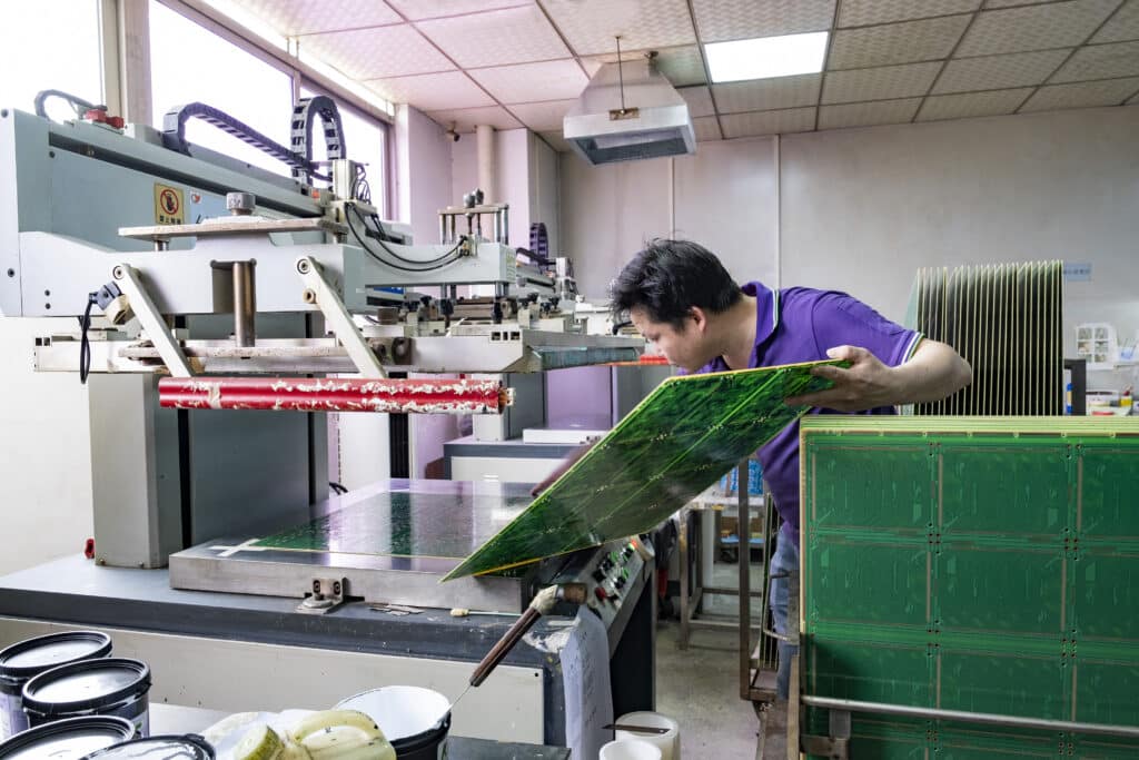
The manual screen printing method is considered the oldest and most cost-effective approach for PCB silkscreen printing. In this process, epoxy ink is manually applied to the laminate and subsequently dried to achieve the desired impression on the PCB. This method is better suited for larger board sizes due to the dominant text size associated with it, requiring sufficient space for the impression to dry effectively. If the objective is to minimize expenses and board spacing is not a constraint, the manual screen printing method can be a viable choice.
Liquid Photo Imaging (LPI)
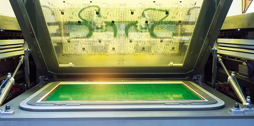
Liquid photo imaging involves coating the laminate with epoxy, which possesses photo imaging properties. The silkscreen sketch is then transferred to plates by exposing them to ultraviolet light. This method yields higher precision compared to the manual silkscreen method and requires less space for implementation. However, it consumes more ink and setup time than alternative screen printing methods. For projects prioritizing PCB space conservation and finer results, the liquid photo imaging method could be an ideal choice.
Direct Legend Printing (DLP)
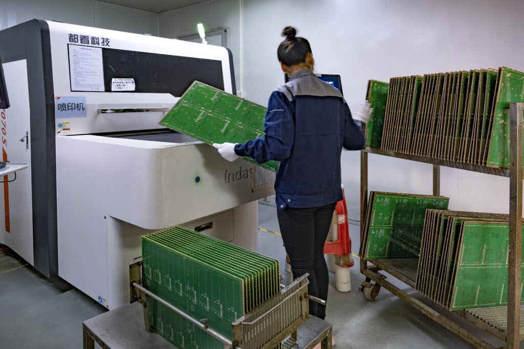
The direct legend printing method employs inkjet printers to transfer ink onto PCBs, similar to how paper printers work. This method allows for direct printing of CAD application information onto the board, offering high accuracy and time efficiency. However, there are limitations to consider with the direct legend printing method. It is not suitable for PCBs made with certain materials, and there may be restrictions on the use of certain types of ink.
In conclusion, the choice of the silkscreen method depends on various factors, including time, price, material, required accuracy, and board spacing. By understanding the advantages and limitations of each method, manufacturers can make informed decisions that best suit their project requirements.
Choosing the Right Silkscreen Method
Selecting the right silkscreen method is a critical step in PCB manufacturing. The choice can significantly impact the quality, cost, and production time of the PCBs. As a PCB & PCBA manufacturer, we at Rowsum have developed a keen understanding of these methods and how to choose the most suitable one for each project.
Factors to Consider
When choosing a silkscreen method, we consider several factors:
- Project Requirements: The complexity and specifications of the project play a significant role in the decision. For instance, projects requiring high precision and fine details might be better suited for methods like Liquid Photo Imaging (LPI) or Direct Legend Printing (DLP).
- Time: The time required for the silkscreen process can impact the overall production timeline. Direct Legend Printing (DLP), for instance, offers high speed and efficiency, making it a good choice for projects with tight deadlines.
- Material Compatibility: Not all methods are suitable for all types of PCB materials. It’s essential to choose a method that is compatible with the specific materials used in the PCB.
Addressing Common Pain Points with Quality Silkscreen
Silkscreen, while often overlooked, can significantly impact the functionality and efficiency of a PCB. Poorly executed silkscreen can lead to several issues, affecting both the manufacturing process and the performance of the final product.
Misidentification of Components
One of the most common issues arising from poor quality silkscreen is the misidentification of components. If the labels on the PCB are unclear or incorrect, it can lead to errors during the assembly process, impacting the functionality of the final product. Clear, accurate, and easy-to-read silkscreen is crucial in preventing such issues.
Inefficient Troubleshooting
A well-executed silkscreen can significantly aid in troubleshooting. If a PCB malfunctions, clear and accurate silkscreen can help identify the issue and expedite repairs. Conversely, poor quality silkscreen can make troubleshooting a time-consuming and frustrating process.
Brand Recognition and Traceability
Silkscreen can also contribute to the brand recognition and traceability of the PCB. A high-quality silkscreen can include the company’s logo, batch numbers for better traceability, and even QR codes for quick access to relevant information. Poor quality silkscreen can result in these important details being unclear or missing entirely.
Component Placement Errors
Poor quality or inaccurate silkscreen can lead to component placement errors during the assembly process. This can result in a malfunctioning PCB and increased time and cost for error correction. A precise and high-quality silkscreen is essential for accurate component placement and efficient assembly.
In conclusion, quality silkscreen is essential in addressing common pain points in PCB manufacturing. It ensures that PCBs are easy to assemble, efficient to troubleshoot, and carry clear identifiers for easy recognition and traceability.
Troubleshooting Guide for Silkscreen in PCBs
While the silkscreen on a PCB might seem like a minor detail, it can have a significant impact on the usability and functionality of the board. Here, we’ll explore some common issues that PCB users might encounter related to the silkscreen.
Illegible or Faded Silkscreen Labels
One of the most common issues that PCB users face is illegible or faded silkscreen labels. This can make it difficult to identify components or understand the layout of the board. The labels might be too small, the ink might not be durable enough, or the contrast between the ink and the PCB material might be too low.
Incorrect or Misleading Silkscreen Labels
Another common issue is incorrect or misleading silkscreen labels. This can lead to confusion or mistakes when assembling or repairing the PCB. The labels might be placed in the wrong location, the text might be mirrored or rotated incorrectly, or the labels might not match the actual components.
Inappropriate Size and Layout
The size and layout of the silkscreen can also cause issues. If the silkscreen is too large, it might take up valuable space on the PCB that could be used for components. If the layout is not well-organized, it might make the PCB difficult to read and understand.
Unsuitable Font and Style
The choice of font and style for the silkscreen can significantly affect its readability. If the font is too small or the style is too complex, it might make the silkscreen difficult to read.
Incorrect Color Choice
The color of the silkscreen can also cause issues. If the color does not contrast well with the PCB material, it might make the silkscreen difficult to see. Additionally, some colors might not be as durable or fade-resistant as others.
Silkscreen Interfering with Components
In some cases, the silkscreen might interfere with the placement or soldering of components. This can be due to the silkscreen extending into pads or holes, or due to the thickness of the silkscreen layer. The ink might not be fully cured, causing it to smear or peel off during assembly, or the ink might be too thick, causing issues with component placement or soldering.
Addressing Silkscreen Issues
If you’re encountering any of these issues, it’s important to communicate with your PCB manufacturer. They can provide a digital copy of the silkscreen layer to help with identifying components and understanding the layout. They can also assist in improving the quality of the silkscreen in future batches to ensure labels are legible and accurate. If the silkscreen is interfering with components, the manufacturer can adjust the silkscreen process to avoid these issues, such as by ensuring that the silkscreen does not extend into pads or holes, and by controlling the thickness of the silkscreen layer.
Conclusion
Silkscreen in PCB manufacturing, while often overlooked, plays a crucial role in the functionality and usability of the final product. From providing essential information about components and their placement to enhancing the aesthetic appeal of the board, the importance of a high-quality silkscreen cannot be overstated.
While there can be challenges in achieving the perfect silkscreen, understanding these common issues and how to address them can go a long way in ensuring a smooth and efficient manufacturing process. Whether it’s choosing the right method of applying silkscreen, addressing common pain points, or keeping an eye on the future of silkscreen in PCB manufacturing, every step contributes to the creation of a PCB that meets the highest standards of quality and performance.
Partner with Rowsum for Your PCB Needs
Ready to experience the difference that a high-quality silkscreen can make in your PCBs? At Rowsum, we’re committed to delivering PCBs that meet the highest standards of quality, reliability, and performance.
Whether you’re looking for PCB manufacturing, PCB assembly, or components sourcing, we have the services to meet your needs. Visit our website to learn more about how we can help you with your PCB needs.