

Introduction
Ever wondered about the significance of copper in your PCB designs? Or why the standard 1 oz copper thickness is a widely accepted norm? These are crucial questions for anyone involved in PCB design or manufacturing.
Copper thickness is a key factor in PCB design, influencing the board’s electrical conductivity, mechanical strength, and heat dissipation. The industry standard is 1 oz, equivalent to 1.37 mils or 34.79 micrometers. This balance between performance and cost makes it suitable for a variety of applications. However, specific design requirements may necessitate adjustments to this thickness.
In this guide, we’ll explore the role of copper in PCBs, decode the standard 1 oz copper thickness, and provide practical tips for tailoring copper thickness to your design needs. Let’s dive in!
The Crucial Role of Copper in PCB
Copper plays an indispensable role in PCB design due to its excellent electrical conductivity. It’s the primary material used for the creation of circuit paths, allowing for efficient transmission of electrical signals across the board. But why copper? Why not any other metal?
Copper’s popularity in PCB design can be attributed to its unique properties. First and foremost, copper has one of the highest electrical conductivity rates among all the metals, second only to silver. This means that copper can transmit electrical signals with minimal loss of energy, ensuring efficient operation of the electronic device.
In addition to its electrical conductivity, copper also has excellent thermal conductivity. This property allows copper to dissipate heat generated by the electronic components, preventing overheating and ensuring the reliability and longevity of the device.
Copper is also highly malleable and ductile, which means it can be easily shaped into thin wires or traces without breaking. This is particularly important in PCB design, where intricate circuit paths need to be created in small spaces.
Finally, copper is relatively abundant and affordable compared to other metals with similar properties, such as silver. This makes copper a cost-effective choice for PCB manufacturing.
Decoding the Standard Copper Thickness in PCB Design
When it comes to copper thickness in PCB design, the term “1 oz copper” is frequently used. But what does this mean? And why is it often the default in the industry?
The term “1 oz copper” refers to the thickness of copper that is achieved when 1 ounce of copper is spread evenly over a one square foot area. This results in a thickness of 1.37 mils, or 34.79 micrometers. This is the default copper thickness used in many PCB designs.
To help you better understand these measurements, here’s a handy conversion table:
| Copper Weight | Thickness in Mils | Thickness in Micrometers | Thickness in Millimeters |
|---|---|---|---|
| 0.5 oz | 0.7 mils | 17.5 µm | 0.0175 mm |
| 1 oz | 1.4 mils | 35 µm | 0.035 mm |
| 2 oz | 2.8 mils | 70 µm | 0.07 mm |
| 3 oz | 4.2 mils | 105 µm | 0.105 mm |
But why this particular thickness? Why not thicker or thinner?
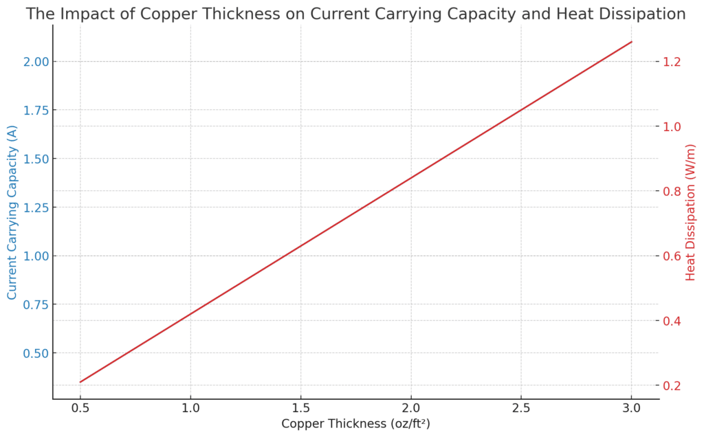
The 1 oz copper thickness is a balance between electrical conductivity and physical durability. Thicker copper layers can carry more current and have better heat dissipation properties. However, they also make the PCB thicker, heavier, and more expensive. On the other hand, thinner copper layers can make the PCB lighter and cheaper, but they may not carry sufficient current for some applications and may be more prone to physical damage.
The 1 oz copper thickness provides sufficient electrical performance for many applications while keeping the PCB relatively thin, light, and cost-effective. It’s a compromise that works well for a wide range of PCB designs.
However, it’s important to note that the 1 oz standard is not a one-size-fits-all solution. It’s the default standard used by manufacturers when a customer doesn’t specify a different thickness. Depending on the specific requirements of your design, you might need to adjust this thickness. In the next section, we’ll discuss how to tailor copper thickness to meet your design needs.
Tailoring Copper Thickness to Meet Design Needs
Designing a PCB is a nuanced process, and the copper thickness is one aspect that may need to be adjusted based on specific design requirements. The key factors to consider when determining the appropriate copper thickness include the amount of current the board needs to carry, the intricacy of the circuit paths, and cost considerations.
To calculate the optimal copper thickness for your PCB, you need to consider the current carrying capacity of the copper traces. This can be determined using the IPC-2221 standard, which provides a formula to calculate the cross-sectional area of the trace required for a given current. The formula is:
A = (I / (k * dT^0.44))^(1/0.725)
where:
- I is the current in amperes,
- k is a constant (0.048 for a trace on the surface of a PCB in free air, or 0.024 for a trace in an internal layer),
- dT is the temperature rise above the ambient temperature in degrees Celsius, and
- A is the cross-sectional area of the trace in square mils.
Let’s consider a practical example to illustrate this calculation. Suppose you’re designing a PCB for a device that requires the board to carry a current of approximately 35 amperes. You want the temperature rise to be no more than 20 degrees Celsius, and you’re using a trace on the surface of the PCB in free air. Plugging these values into the formula, we get:
A = (35 / (0.048 * 20^0.44))^(1/0.725) A = 265.2 square mils
This is the required cross-sectional area of the trace. To convert this to copper thickness, you would divide by the width of the trace. For instance, if the trace is 0.100 inches (100 mils) wide, the required copper thickness would be 265.2 / 100 = 2.652 mils.
However, PCB manufacturers typically specify copper thickness in ounces per square foot (oz/ft²), not mils. To convert from mils to oz/ft², you can use the fact that 1 oz/ft² is approximately equal to 1.37 mils. So:
Copper thickness = 2.652 mils / 1.37 (mils/oz) = 1.94 oz
This value is slightly lower than the standard 2 oz/ft² but falls within the typical range for PCBs, which is from 0.5 oz/ft² to 2 oz/ft². In this case, you might consider specifying a copper thickness of 2 oz/ft² for your PCB to ensure it can handle the required current.
The intricacy of your circuit design is another crucial factor. If your design includes detailed circuit paths or small features, a thinner copper layer may be necessary to achieve the required precision. However, bear in mind that thinner layers are more delicate and may require careful handling during the manufacturing process.
Lastly, cost considerations play a significant role. Thicker copper layers require more material, making them more expensive to manufacture. Balancing the technical requirements of your design with cost considerations is crucial to achieving an optimal design.
By understanding these factors and how to calculate the appropriate copper thickness, you can tailor your PCB design to meet its specific needs, ensuring optimal performance and reliability.
Copper Thickness and Spacing Rules in PCB Design
Copper thickness and spacing are two critical parameters in PCB design that directly impact the board’s performance and reliability. They are interrelated, and understanding their relationship is crucial for achieving optimal design outcomes.
Copper Thickness and Its Impact
The copper thickness on a PCB determines the amount of current that the traces can carry without overheating. It also affects the board’s impedance, a critical factor in high-speed and RF designs. The standard copper thickness used in the industry is 1 oz/ft², which is approximately 1.37 mils or 34.79 micrometers. However, depending on the application, the copper thickness can be increased to 2 oz/ft² or even higher.
Spacing Rules and Their Importance
The spacing between the copper features on a PCB, such as traces and pads, is equally important. It must be sufficient to prevent electrical shorts and to withstand the voltage levels in the circuit. The required spacing can vary depending on factors such as the operating voltage and the environment in which the PCB will be used.
The IPC-2221 standard provides guidelines for determining the minimum spacing based on the peak working voltage. For instance, for a peak voltage of up to 50V, a spacing of 0.005″ (5 mils) is recommended.
Balancing Copper Thickness and Spacing
In PCB design, balancing copper thickness and spacing is a delicate act. Increasing the copper thickness allows the board to carry more current, but it also requires larger spacing between the copper features, which can be a challenge in high-density designs.
Conversely, reducing the copper thickness allows for smaller spacing and higher density, but it also reduces the current-carrying capacity of the traces. Therefore, the designer must carefully consider both factors and make trade-offs as necessary to meet the design requirements.
In conclusion, understanding and correctly applying the rules for copper thickness and spacing is essential for designing reliable and efficient PCBs. It’s always recommended to check with your PCB manufacturer for their specific capabilities and guidelines, as these can vary.
| Copper Weight | Min. Recommended Space and Min. Trace Width (mils) | Min. Recommended Space and Min. Trace Width (mm) |
|---|---|---|
| 1 oz | 3.5 mils | 0.089 mm |
| 2 oz | 8 mils | 0.203 mm |
| 3 oz | 10 mils | 0.254 mm |
| 4 oz | 14 mils | 0.355 mm |
Tips for Applying the Proper Copper Thickness
Choosing the right copper thickness for your PCB design is crucial, but it’s not the only consideration. Here are some additional tips to help you apply the proper copper thickness in your designs:
1. Distribute Your Copper as Evenly as Possible:
When designing a PCB, aim to spread your copper as evenly as possible across each layer. This is particularly important in complex multi-layer designs, such as an 8-layer PCB for a high-speed communication device. The plating and etching processes used in PCB manufacturing can affect different areas of the board at slightly different rates. By distributing the copper evenly, you can help ensure a more uniform result.
2. Balance Copper Weight Across All Layers:
It’s generally best to use the same copper weight across all layers of your PCB. For instance, if you’re designing a 4-layer PCB for a compact IoT device, you might choose to use 1 oz/ft² copper on all layers. This helps maintain a balanced structure, reducing the risk of warping or twisting under high operating temperatures or during the assembly process.
3. Match Copper Weight on Outer Layers:
The top and bottom layers of your PCB should have the same copper weight. This is because these layers are processed together during etching. For example, if you’re designing a double-sided PCB for a power supply unit and you’re using 2 oz/ft² copper on the top layer, you should also use 2 oz/ft² on the bottom layer to avoid over-etching.
4. Consider the Impact on Trace Spacing:
Remember that increasing the copper thickness can also affect the minimum spacing between traces. For instance, if you’re designing a high-current PCB for an electric vehicle charger and you’re increasing the copper weight from 1 oz/ft² to 2 oz/ft², you might need to increase the trace spacing from 3.5 mils to 8 mils to avoid any potential issues.
5. Always Specify Your Requirements:
Don’t assume that your PCB manufacturer will know what copper thickness you need. Always specify your requirements clearly in your design files or fabrication notes. For example, if you’re designing a PCB for a high-frequency radar system that requires 3 oz/ft² copper, be sure to state this explicitly in your design documentation.
By keeping these tips in mind, you can make more informed decisions about the copper thickness in your PCB designs and achieve better results.
Conclusion
Designing a PCB involves a multitude of decisions, and choosing the right copper thickness is a critical one. It’s a decision that impacts the PCB’s performance, cost, and manufacturability. Whether you’re designing a simple gadget or a complex medical device, understanding and applying the principles of copper thickness can make a significant difference.
Remember, the right copper thickness can help you balance electrical requirements, durability, and cost-effectiveness. It’s not just about following industry standards, but about understanding your specific needs and making informed decisions.
At Rowsum, we understand these complexities and are committed to helping you navigate through them. As a leading PCB manufacturer, we offer tailored solutions to meet your unique requirements. Our team of experts is always ready to provide guidance and support, ensuring you get the best out of your PCB designs.
If you have any questions or need further assistance with your PCB designs, feel free to reach out to us at [email protected]. Visit us at www.rowsum.com to learn more about our services and how we can help you succeed in your PCB projects.