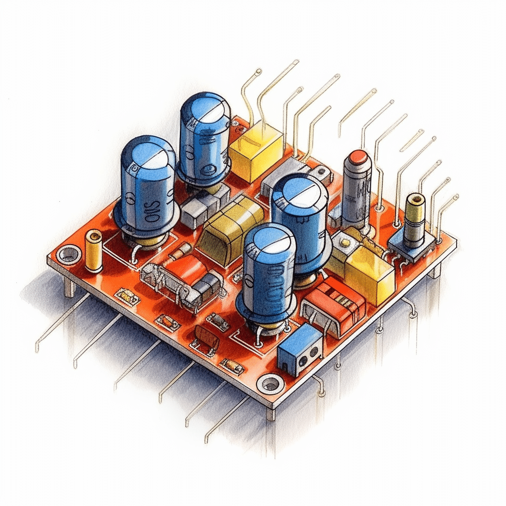
Introduction
Have you ever found yourself lost in the sea of acronyms and technical jargon when diving into the world of Printed Circuit Board Assembly (PCBA)? Ever wondered what SMT, PTH, or BGA stand for? Or perhaps you’ve been puzzled by terms like ‘reflow soldering’, ‘wave soldering’, or ‘selective soldering’? You’re not alone. The world of PCBA is filled with specialized terminology that can be overwhelming for both beginners and seasoned professionals alike.
In this comprehensive guide, we aim to demystify the complex language of PCBA. We will dive into the most common, as well as some of the more obscure, terms used in the industry. From design to components, assembly processes to soldering techniques, and quality compliance to failure analysis – we’ve got you covered.
Stay with us as we embark on this enlightening journey through the most detailed and complete PCBA terminology guide of 2023. This is your one-stop resource to becoming fluent in the language of PCBA.
PCBA Design Terminology
Basic Design Terms
- Schematic Design: The schematic design is the initial design stage where the circuit is represented in a simplified manner. It includes the representation of components and their interconnections.
- PCB Layout Design: PCB layout design is the process of placing and routing all the components on the PCB. It involves deciding where and how components should be placed, routing the electrical connections between them, and optimizing the layout for best performance.
- Gerber Files: Gerber files are the standard file format used by PCB manufacturers to understand the design of the PCB. They contain information about the copper layers, solder mask, silkscreen, and drill data.
- Bill of Materials (BOM): The BOM is a list of all the components that will be placed on the PCB. It includes information such as the component’s manufacturer, part number, quantity, and placement location on the board.
- Design for Manufacturing (DFM): DFM is a set of guidelines that designers follow to ensure that their PCB design can be easily and reliably manufactured.
- Design for Assembly (DFA): DFA is a set of guidelines that designers follow to ensure that their PCB design can be easily and efficiently assembled.
- Design for Test (DFT): DFT is a set of guidelines that designers follow to ensure that their PCB design can be easily and effectively tested.
- CAD (Computer-Aided Design): CAD software is used by designers to create the schematic and layout designs of the PCB.
- DRC (Design Rule Check): DRC is a process in which a software tool checks a PCB layout to ensure it meets the design rules for minimum trace width, minimum spacing between traces, etc.
Advanced Design Terms
- High-Speed Design: High-speed design is a specialized area of PCB design where the signal integrity, power integrity, and electromagnetic compatibility of the PCB are carefully considered due to the high operating frequencies.
- RF (Radio Frequency) Design: RF design is a specialized area of PCB design where the PCB is designed to operate with signals in the radio frequency range (3 kHz to 300 GHz).
- Mixed-Signal Design: Mixed-signal design is a type of PCB design that involves both analog and digital circuits.
- Flex and Rigid-Flex Design: Flex and rigid-flex design involves designing PCBs that are flexible or a combination of rigid and flexible.
- HDI (High-Density Interconnect) Design: HDI design involves designing PCBs that have a higher wiring density per unit area compared to conventional PCBs.
- MCAD (Mechanical Computer-Aided Design): MCAD software is used in conjunction with electrical CAD software for designing PCBs to ensure the PCB fits into the final product enclosure and meets all mechanical constraints.
- ECAD (Electrical Computer-Aided Design): ECAD software is used for creating the schematic design and PCB layout design.
- DFX (Design for Excellence): DFX is a comprehensive set of guidelines that includes DFM, DFA, DFT, and other considerations to ensure the PCB design is optimal in all aspects.
PCBA Components Terminology
Basic Components
- Resistor (R): A resistor is a passive two-terminal electrical component that implements electrical resistance as a circuit element. Common packages include 0201, 0402, 0603, 0805, 1206, and so on.
- Capacitor (C): A capacitor is a passive two-terminal electronic component that stores electrical energy in an electric field. Common packages include 0201, 0402, 0603, 0805, 1206, and so on.
- Inductor (L): An inductor, also called a coil or reactor, is a passive two-terminal electrical component that stores energy in a magnetic field when electric current flows through it. Common packages include 0201, 0402, 0603, 0805, 1206, and so on.
- Diode (D): A diode is a two-terminal electronic component that conducts current primarily in one direction. Common packages include SOD-123, SOD-323, SOD-523, SOD-723, etc.
- Transistor (Q): A transistor is a semiconductor device used to amplify or switch electronic signals and electrical power. Common packages include TO-92, TO-220, SOT-23, SOT-223, etc.
Advanced Components
- Integrated Circuit (IC): An integrated circuit or monolithic integrated circuit is a set of electronic circuits on one small flat piece of semiconductor material, usually silicon. Common packages include DIP, QFP, BGA, SOP, SSOP, TSSOP, etc.
- Microcontroller (U): A microcontroller is a small computer on a single integrated circuit containing a processor core, memory, and programmable input/output peripherals. Common packages include DIP, QFP, BGA, SOP, SSOP, TSSOP, etc.
- Operational Amplifier (Op-Amp, U): An operational amplifier is a high-gain voltage amplifier with a differential input and, usually, a single-ended output. Common packages include DIP, SOIC, MSOP, etc.
- Digital to Analog Converter (DAC, U): A DAC is a system that converts a digital signal into an analog signal. Common packages include DIP, SOIC, MSOP, etc.
- Analog to Digital Converter (ADC, U): An ADC is a system that converts an analog signal, such as a sound picked up by a microphone or light entering a digital camera, into a digital signal. Common packages include DIP, SOIC, MSOP, etc.
Additional Components
- Battery (BT): A battery is a device consisting of one or more electrochemical cells with external connections for powering electrical devices.
- Speaker (SP): A speaker is an electroacoustic transducer which converts an electrical audio signal into a corresponding sound.
- Microphone (M): A microphone is a device that captures audio by converting sound waves into an electrical signal.
- Motor (M): A motor is a machine that converts electrical energy into mechanical energy.
- Display (DS): A display is an output device for presentation of information in visual or tactile form.
- Thermistor (TH): A thermistor is a type of resistor whose resistance is dependent on temperature.
- Photodiode (PD): A photodiode is a semiconductor device that converts light into an electrical current. Common packages include TO-18, TO-46, TO-5, etc.
- Phototransistor (Q): A phototransistor is a semiconductor device that is used to detect light and convert it into an electrical signal. Common packages include TO-18, TO-46, TO-5, etc.
- Voltage Regulator (VR): A voltage regulator is a system designed to automatically maintain a constant voltage level. Common packages include TO-220, TO-252 (DPAK), TO-263 (D2PAK), SOT-223, etc.
- RF Module (RF): An RF module is a small electronic device used to transmit and/or receive radio signals between two devices.
- Memory Chip (U): A memory chip is an electronic data storage medium that uses integrated circuit technology to store information. Common packages include DIP, SOP, SSOP, TSSOP, etc.
- Clock Generator (CLK): A clock generator is a circuit that produces a timing signal for use in synchronizing a circuit’s operation. Common packages include DIP, SOP, SSOP, TSSOP, etc.
PCBA Assembly Process Terminology
- SMT (Surface Mount Technology): SMT is a method for producing electronic circuits in which the components are mounted or placed directly onto the surface of printed circuit boards (PCBs).
- Through-Hole Technology (THT): THT is a method of fitting components with wire leads into holes drilled in the circuit board.
- Pick and Place Process: This is the process of placing components on the PCB using a pick and place machine.
- Reflow Soldering: Reflow soldering is a process in which a solder paste (a sticky mixture of powdered solder and flux) is used to temporarily attach one or several electrical components to their contact pads.
- Wave Soldering: Wave soldering is a bulk soldering process used in the manufacture of printed circuit boards.
- Hand Soldering: Hand soldering is done for parts that cannot be soldered by machines, like large, bulky components, or for prototypes.
- Inspection Methods: This includes visual inspection, automated optical inspection (AOI), and X-ray inspection. These methods are used to ensure the quality of the PCBs after assembly.
- Functional Test (FCT): Functional testing is a quality assurance process and a type of black-box testing that bases its test cases on the specifications of the software component under test.
- Conformal Coating: Conformal coating is a protective chemical coating or polymer film 25-75µm thick (50µm typical) that ‘conforms’ to the circuit board topology.
- Box Build Assembly: Box build assembly, also known as systems integration, is an assembly work other than a printed circuit board (PCB) production. It is an electromechanical assembly process, which includes enclosure fabrication, installation and routing of cabling or wire harnesses, and installation of sub-assemblies and components.
- Rework/Repair: Rework/repair involves the process of rectifying errors on the PCB after assembly.
- Depaneling: Depaneling is the process of removing the individual PCBs from the panel they were assembled on.
PCBA Soldering Techniques Terminology
Basic Soldering Techniques
- Wave Soldering: This is a large-scale soldering process by which electronic components are soldered to a PCB to form an electronic assembly. The name is derived from the use of waves of molten solder to attach metal components to the PCB. The process uses a tank to hold a quantity of molten solder; the components are inserted into or placed on the PCB and the loaded PCB is passed across a pan of molten solder. The solder sticks to the exposed metallic areas of the board (those not protected with solder mask), creating a reliable mechanical and electrical connection.
- Reflow Soldering: Reflow soldering is a process in which a solder paste (a sticky mixture of powdered solder and flux) is used to temporarily attach one or thousands of tiny electrical components to their contact pads, after which the entire assembly is subjected to controlled heat. The solder paste reflows in a molten state, creating permanent solder joints. Heating may be accomplished by passing the assembly through a reflow oven or under an infrared lamp or by soldering individual joints with a hot air pencil.
- Selective Soldering: Selective soldering is the process of selectively soldering components to printed circuit boards and molded modules that could be damaged by the heat of a reflow oven or wave soldering in a traditional surface-mount technology (SMT) assembly process. This usually follows an SMT oven reflow process; parts to be selectively soldered are usually surrounded by SMT components, and the process is controlled carefully using flux and other means to prevent the nearby components from reflowing again.
- Hand Soldering: Hand soldering is done with a soldering iron or soldering station. It’s a manual process typically used for small-scale production or prototyping.
Advanced Soldering Techniques
- Hot Bar Soldering: Hot Bar Soldering is a selective soldering process where two pre-fluxed, solder coated parts are heated to a temperature sufficient to cause the solder to melt, flow, and then solidify, forming a permanent electromechanical bond between the parts. Hot Bar Soldering is highly repeatable, efficient, and requires no consumables.
- Infrared Soldering: Infrared Soldering is a process that uses infrared radiation to heat the joint to be soldered. The radiation is absorbed by the joint and is then converted into heat. This method is often used in automated processes and is suitable for both through-hole and surface mount technology.
- Vapor Phase Soldering: Vapor Phase Soldering is a process that uses a vapor phase machine which creates a vapor from a liquid with a specific boiling point. The PCB is heated by condensation of the vapor on the PCB surface. This method provides very even heating and is especially useful for complex boards.
- Laser Soldering: Laser Soldering is a non-contact process that uses a laser to generate the heat required for soldering. This method is highly accurate and can be used for small, delicate parts.
- Induction Soldering: Induction Soldering is a process that produces heat by passing an electrical current through a coil. The heat is generated by the resistance to the current within the coil. This method is often used for soldering wires and other small components.
- Resistance Soldering: Resistance Soldering is a process where heat is generated by passing a current through a resistive material. In this process, the heat is generated at the joint, reducing the risk of thermal damage to the PCB.
- Oven Reflow Soldering: Oven Reflow Soldering is a process in which a solder paste is used## PCBA Soldering Techniques Terminology.
PCBA Testing and Inspection Terminology
Basic Testing and Inspection Terms
- Visual Inspection: This is the most basic form of PCB inspection, where the board is visually examined for obvious flaws like missing components or broken traces.
- Automated Optical Inspection (AOI): AOI is a non-contact test method that uses a high-speed camera and light to capture images of the PCB. These images are then compared to a digital image of a “good” board to identify any defects.
- X-Ray Inspection: This method uses X-rays to inspect the internal features of the PCB, such as the quality of solder joints under a BGA (Ball Grid Array) package.
- In-Circuit Test (ICT): ICT is a method of testing where probes are used to check the operation of components on a PCB. This test can detect problems like shorts, opens, resistance, capacitance, and other basic quantities.
- Functional Test (FCT): FCT is a type of black-box testing where the functionality of the PCB is tested under simulated operating conditions.
Advanced Testing and Inspection Terms
- Boundary Scan (JTAG): Boundary Scan is a method for testing interconnects on PCBs or sub-blocks inside an integrated circuit. It is also known as JTAG (Joint Test Action Group).
- Flying Probe Test: This is a type of ICT that doesn’t require a test fixture. It uses moving probes to test electrical performance of components and solid connections.
- Automated X-ray Inspection (AXI): AXI is a technology based on the same principles as simple X-ray inspection, but with automation to allow testing of complex PCBs.
- Thermal Imaging: This method uses a thermal camera to detect hot spots on a PCB, which can indicate areas of high resistance or components that are consuming more power than expected.
- Signal Integrity Analysis: This is a measure of the quality of an electrical signal. In the context of PCB testing, signal integrity analysis can be used to detect issues like crosstalk, signal reflection, and signal loss.
- Power Integrity Analysis: This is a measure of how well a system converts and delivers power from the source to the load without degrading signal integrity. In the context of PCB testing, power integrity analysis can be used to detect issues like voltage drops, power supply noise, and ground bounce.
PCBA Failure Analysis Terminology
Common Failure Modes
- Open Circuit: An open circuit is a type of failure where a break in the circuit prevents current from flowing. This could be due to a broken trace, a failed solder joint, or a component failure.
- Short Circuit: A short circuit is a type of failure where an unintended connection is made between two points in the circuit, causing current to flow in an undesired path. This could be due to a solder bridge, a component failure, or damage to the PCB.
- Component Failure: Component failure refers to any situation where a component on the PCB fails to perform its intended function. This could be due to a manufacturing defect, improper handling, or operating the component outside its specified conditions.
- Solder Joint Failure: Solder joint failure refers to any situation where a solder joint on the PCB fails to maintain a reliable electrical connection. This could be due to a variety of factors, including poor soldering technique, mechanical stress, or thermal cycling.
- Pad Lift: Pad lift is a type of failure where the copper pad on the PCB separates from the underlying substrate. This can be caused by mechanical stress or excessive heat during soldering.
- Trace Damage: Trace damage refers to any situation where a copper trace on the PCB is damaged or broken. This can be caused by physical damage to the PCB, excessive current, or corrosion.
Failure Analysis Techniques
- Visual Inspection: Visual inspection is the process of examining the PCB and its components with the naked eye or with the aid of a microscope to identify any visible defects or anomalies.
- X-Ray Inspection: X-ray inspection is a non-destructive testing technique that uses x-rays to view the internal structures of the PCB and its components. This can be useful for identifying hidden defects such as solder bridges or voids in BGA solder joints.
- Microsectioning: Microsectioning is a destructive testing technique that involves cutting a cross-section of the PCB for detailed examination under a microscope. This can provide valuable information about the internal structures of the PCB and its components.
- Electrical Testing: Electrical testing involves applying signals to the PCB and measuring its response to verify its functionality and identify any faults.
- Thermal Cycling: Thermal cycling is a testing technique that involves repeatedly heating and cooling the PCB to simulate the thermal stresses it may experience during its lifetime. This can help to identify any weaknesses or defects that may lead to failure over time.
- Failure Mode and Effects Analysis (FMEA): FMEA is a systematic process for identifying potential failure modes, determining their effects on the system, and prioritizing actions to mitigate those failures.
Conclusion
Navigating the world of PCBA can be a complex task, with a multitude of terms and concepts to understand. However, with this comprehensive guide to PCBA terminology, we hope to have illuminated some of the key terms and concepts that you will encounter in this field. Whether you are a seasoned professional looking to refresh your knowledge, or a newcomer to the field, understanding these terms is crucial to your success in the world of PCBA.
At Rowsum, we understand the importance of clear and accurate communication in delivering high-quality PCBA services. Our team of experts is always ready to assist you with any questions or concerns you may have about your PCBA projects. We pride ourselves on our commitment to quality, precision, and customer satisfaction. For more information about our services, or to start your journey with us, visit: www.rowsum.com.
FAQs
Q1: What is the difference between PCB and PCBA?
A: PCB stands for Printed Circuit Board, which is the board itself without any components. PCBA stands for Printed Circuit Board Assembly, which refers to the PCB with all the components soldered onto it.
Q2: What is a SMT in PCBA?
A: SMT stands for Surface Mount Technology. It is a method for producing electronic circuits in which the components are mounted directly onto the surface of PCBs.
Q3: What is the role of solder paste in PCBA?
A: Solder paste is used in the assembly process to solder surface-mount components to the PCB. It is a mixture of tiny solder particles and flux.
Q4: What is a BOM in PCBA?
A: BOM stands for Bill of Materials. It is a list of all the components used in a PCB design, including information such as the component designators, part numbers, quantities, and descriptions.
Q5: What is meant by ‘trace’ in PCBA?
A: A trace is a continuous path of copper on a PCB that electrically connects different components.
Q6: What is the purpose of a via in PCBA?
A: A via is a small hole in a PCB that is plated with metal to create an electrical connection between different layers of the board.
Q7: What is the significance of ‘clearance’ in PCBA?
A: Clearance refers to the minimum distance required between different electrical objects on the PCB to prevent electrical shorting and interference.
Q8: What is meant by ‘component placement’ in PCBA?
A: Component placement refers to the positioning of components on the PCB layout. Proper component placement can have a significant impact on the performance of the final product.
Q9: What is the role of a ‘solder mask’ in PCBA?
A: Solder mask is a protective layer applied to the bare board to prevent solder bridging between closely spaced pads and to protect the copper from corrosion.
Q10: What is ‘panelization’ in PCBA?
A: Panelization is a technique used in PCB manufacturing where multiple boards are fabricated as a single unit to improve manufacturing efficiency.
For more detailed information and further queries, don’t hesitate to visit us at: www.rowsum.com.