1. Introduction
1.1 Brief of PCB and PCBA
In our digitally interconnected world, the hidden wizards that keep our devices ticking are PCBs and PCBAs. As integral components of nearly every electronic device we use daily – from the humble alarm clock to our smartphones, computers, and even high-tech drones – understanding the nuts and bolts of Printed Circuit Boards (PCB) and Printed Circuit Board Assembly (PCBA) can be truly enlightening.
But what exactly are PCBs and PCBAs? How do they breathe life into the gadgets we take for granted? By unraveling these seemingly complex concepts, you can not only gain a deeper appreciation for the everyday marvels of technology but also make informed decisions if your work or interests ever intersect with these intricate, essential components.
So, are you ready to embark on a fascinating journey into the world of PCBs and PCBAs, exploring their intricate layers, understanding the significance of solder masks, diving into the materials that build them, and finally, understanding how to navigate the procurement process like a pro? Let’s get started! This guide promises to be the most comprehensive introduction to PCB and PCBA you’ll find on the internet. Buckle up, and let’s dive in!
2. In-Depth Understanding of PCB
The intricate world of PCBs is a testament to how far electronics have come. Delving deep into this topic will not only enhance your understanding of modern technology but also equip you with valuable knowledge about the hidden heroes in every electronic device.
2.1. Basic Knowledge about PCB
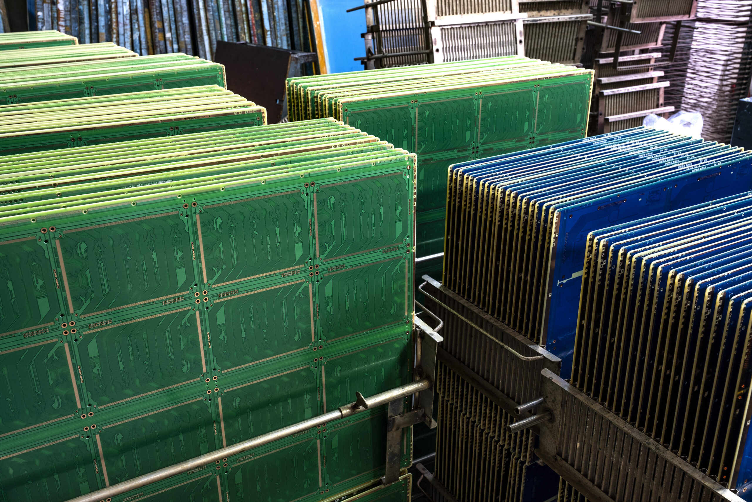
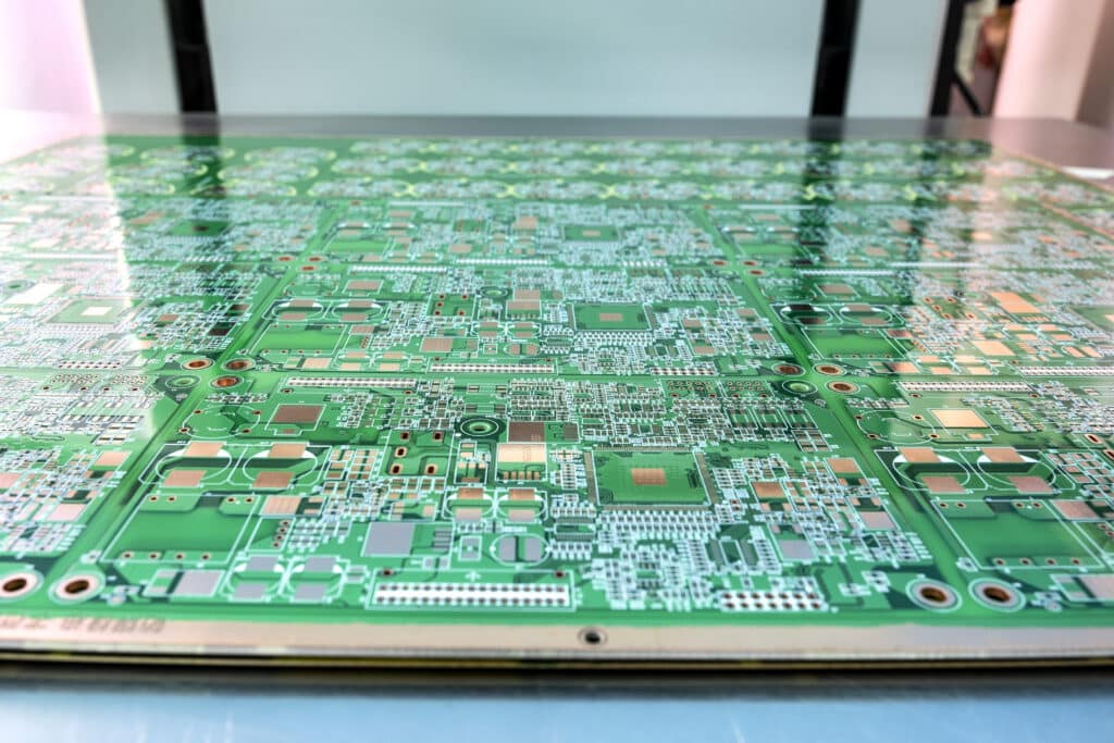
Printed Circuit Boards, or PCBs, are thin boards made from an insulating material, coated with conductive material on both or either side. They play a pivotal role in connecting various electronic components through etched pathways, thus creating a circuit. These boards are widely used in almost all electronic devices, ranging from your mobile phones and laptops to industrial machinery and healthcare equipment.
2.2. Layers in PCB
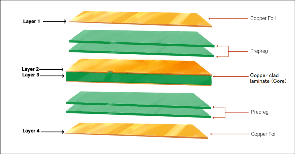
PCBs are categorized based on the number of conductive layers, which include single-sided (one layer), double-sided (two layers), and multi-layer (three or more layers). Each layer carries different parts of the circuit and communicates with other layers through small holes called “vias.”
- Single-sided PCBs have the conductive material applied only on one side.
- Double-sided PCBs have conductive material on both sides of the board.
- Multi-layer PCBs consist of three or more layers of conductive material that are laminated together under high temperature and pressure. These are often used in high-density and complex electronic circuits.
2.3. Understanding Solder Resist (Solder Mask)
A solder mask, also known as a solder resist, is a layer of insulating material applied to the PCB’s surface. Its primary function is to protect the copper traces from oxidation, provide electrical insulation, and prevent solder bridges from forming during the soldering process. This layer is usually green but can also come in different colors like blue, red, or black.
2.4. Materials Used in PCB
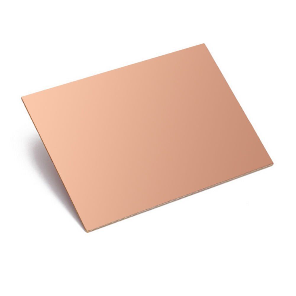
PCBs are predominantly made from fiberglass, specifically FR4 (Flame Retardant 4), which provides a high level of strength and durability. Other materials include copper, which forms the conductive pathways, and a solder mask, which provides insulation. The choice of materials often depends on the complexity and requirements of the specific device in which the PCB will be used.
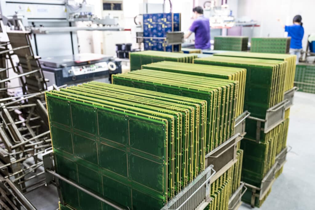
2.5. PCB Fabrication Process
An integral part of understanding PCB basics involves familiarizing oneself with the PCB fabrication process. This process involves several steps that require careful attention to detail and precision. It’s in these steps that the various PCB surface finish methods come into play. Here, we will explore some of the most common PCB fabrication methods:
- 1. Lead-Free HASL (Hot Air Solder Leveling): As the push towards environmentally friendly practices in the electronics industry continues, lead-free HASL has become increasingly popular. This process involves applying molten tin-lead solder to the PCB followed by hot air blowing to level and remove excess solder. The result is a very reliable and cost-effective finish.
- 2. OSP (Organic Solderability Preservative): OSP is a water-based, organic surface finish that is selectively applied to bare copper. It works by placing a protective layer over the copper to prevent it from oxidizing and maintaining its solderability. This process is environmentally friendly and allows for easy reworking of PCBs.
- 3. ENIG (Electroless Nickel Immersion Gold): This surface finish involves depositing an initial layer of nickel onto the copper, followed by a thin layer of immersion gold. ENIG provides excellent surface planarity and is highly suited for dense, flat PCBs. It is particularly favored for its excellent shelf life and good corrosion resistance.
- 4. Immersion Silver: This is a straightforward process where a thin layer of silver is deposited directly onto the copper. Immersion Silver finish is chosen for its low cost, good solderability, and strong adherence to the compliance for RoHS.
- 5. Immersion Tin: This finish involves depositing a flat layer of tin directly onto the copper. Known for its excellent surface planarity, it’s often used for fine pitch technology and press-fit pin insertion.
- 6. Hard Gold Plating: This finish involves plating the copper with a layer of hard gold over a nickel layer. This finish is most commonly used for edge connectors due to its high wear resistance.
Understanding these various fabrication methods gives a comprehensive overview of the options available when designing and manufacturing PCBs, which in turn can significantly impact the performance, cost, and reliability of the final product.
Remember that each method has its own set of advantages and disadvantages, and the choice often depends on the application, environmental conditions, and cost considerations.
Your preferred PCB manufacturer, like Rowsum, can provide further guidance based on the specifics of your project. They would have expertise on the different fabrication methods, ensuring you make the best choice for your PCB needs.
Get Access Now: Rowsum
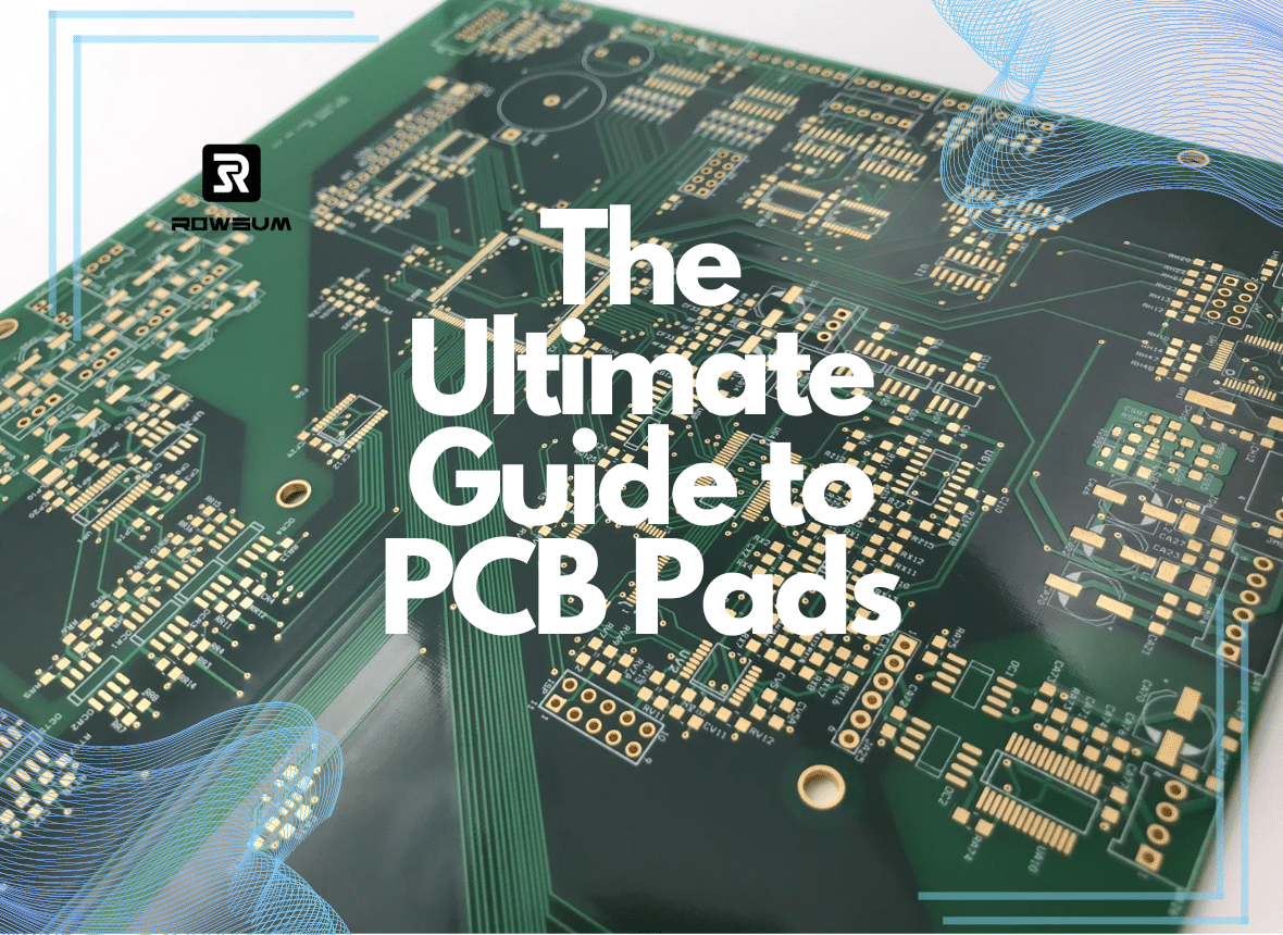
2.6. Pads in PCB

Pads are small areas of copper on a PCB where the pins of the components are soldered. There are two types of pads: through-hole pads, which have holes for components with leads to be inserted, and surface mount pads, which allow components to be placed directly on the surface of the board.
2.7. Expanded Common Terminologies in PCB
To further your understanding of PCBs, let’s look at some more frequently used terms in the industry:
- Finger: These are gold-plated terminals that extend along the edge of a PCB. They’re often used as a point of interface with other PCBs.
- Annular Ring: The copper ring surrounding the drilled holes on a PCB is known as the annular ring.
- Land: It’s another term for pad, the area where a component is soldered onto the PCB.
- Slots: These are non-round holes or cut-outs in the PCB, often used for mounting the board or allowing for components that need additional clearance.
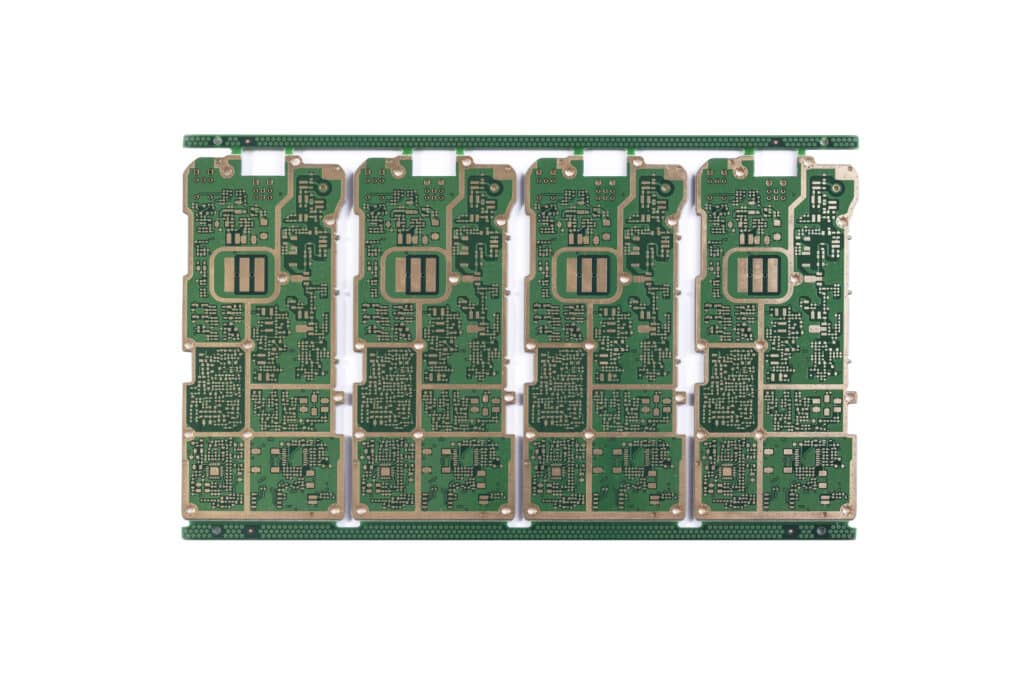
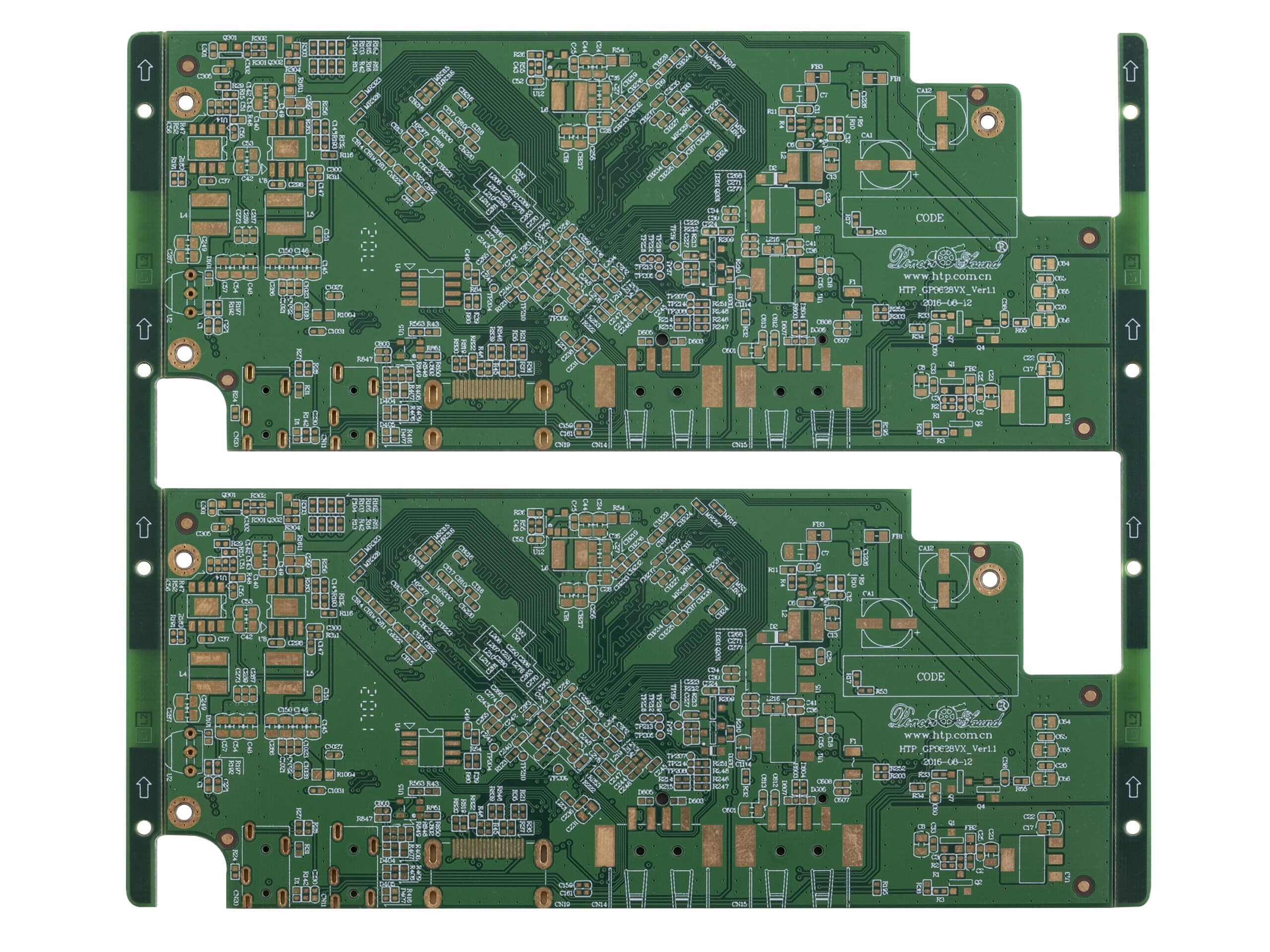
- Array: It refers to a grouping of smaller PCBs on a larger panel, making it easier to handle during assembly.
- Pitch: The term is used to describe the distance from the center of one component to the center of the next component.
- Substrate: The insulating material that forms the bulk of the PCB.
- Plane: A larger section of exposed copper on a PCB, typically connected to either power or ground.
- Gerber Files: These are standard data files containing information about the PCB’s design. They’re used in the manufacturing process.
- DRC (Design Rule Check): A software check to ensure the layout of the PCB doesn’t have any errors like traces being too close together or drill holes being too small.
These are just a few of the commonly used terms you’ll encounter when delving into the realm of PCBs. They provide a glimpse into the intricacies that go into creating these foundational elements of all electronic devices.
3. Types of PCBs
Understanding the diverse types of PCBs used across various industries is fundamental to fully grasping the world of PCBs. Here are some of the common types of PCBs you’ll encounter:
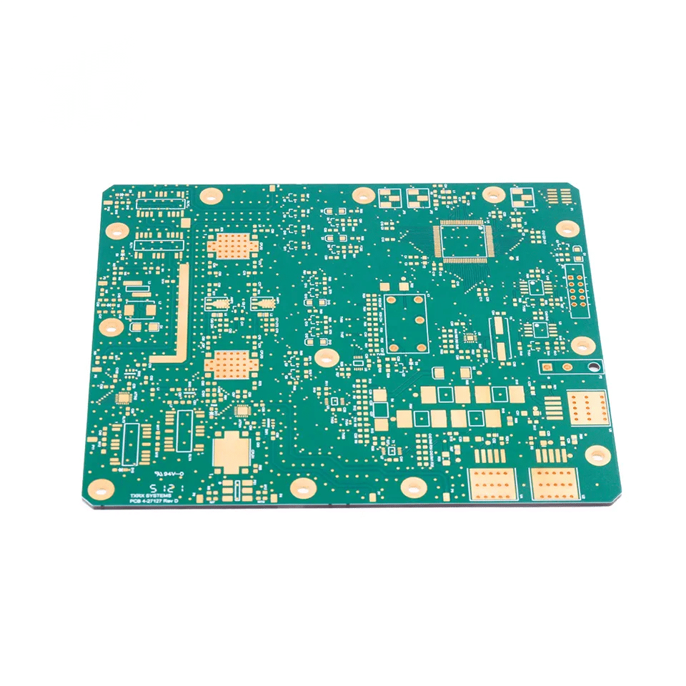
3.1. FR-4 PCBs
These are by far the most commonly used type of PCBs in the electronics industry. The term FR-4 stands for “Flame Retardant 4,” and it is a type of substrate material made from woven fiberglass cloth and epoxy resin. FR-4 PCBs are well-loved for their affordability, availability, and superior electrical properties, making them suitable for a broad range of applications.
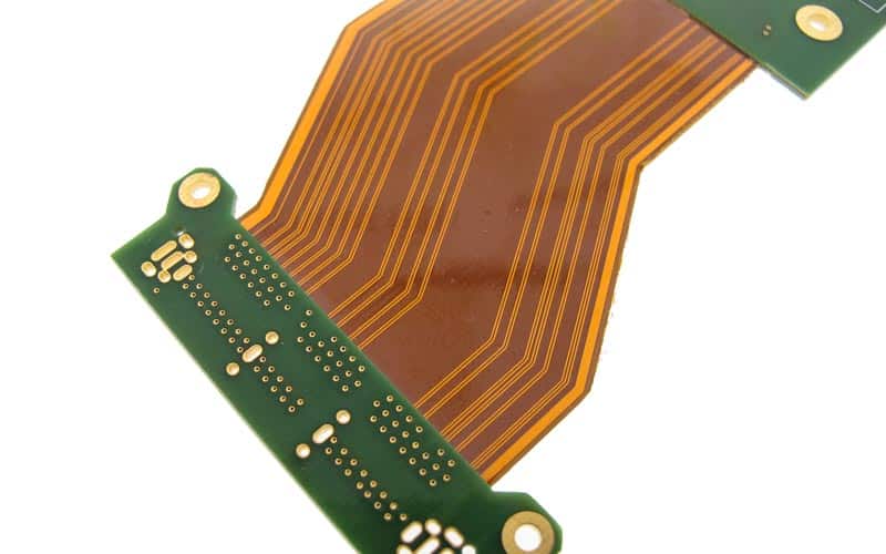
3.2. Flexible PCBs (FPC)
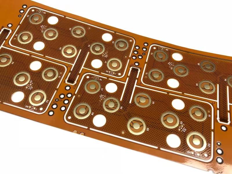
Flexible PCBs, or FPCs, are just what their name suggests — flexible! Unlike rigid FR-4 PCBs, FPCs can bend and flex while maintaining the integrity of their electrical connections. This property makes them incredibly useful in applications where space constraints or movement is involved, such as in smartphones, wearable devices, and automotive applications.
3.3. Aluminum-Backed PCBs
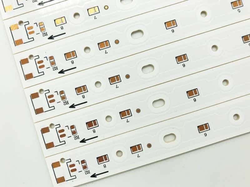
Aluminum-backed PCBs have a unique construction compared to FR-4 and FPCs. The base material in these boards is aluminum, which acts as a heat sink for dissipating the heat produced by the circuit. This makes them an excellent choice for high-power, high-temperature applications such as LED lighting and power supplies.
3.4. High-Frequency PCBs
These types of PCBs are designed specifically to perform reliably in conditions of high-frequency electronic signals, beyond the capacity of regular PCBs. They use specialized materials like Teflon to minimize signal loss and maintain the integrity of signals operating in the gigahertz range.
3.5. Rigid-Flex PCBs
Rigid-flex PCBs combine the best of both worlds from rigid FR-4 PCBs and flexible FPCs. These boards feature regions of rigid PCB for components that need a solid base, and flexible sections where bending and movement are necessary.
Understanding these different types of PCBs can help you appreciate the diverse range of technologies and materials used in PCB design and manufacturing, each with their unique applications and advantages.
These are just a few of the commonly used terms you’ll encounter when delving into the realm of PCBs. They provide a glimpse into the intricacies that go into creating these foundational elements of all electronic devices. In the next section, we’ll continue our deep dive into the world of PCBAs.
I appreciate your feedback. Let’s enhance those points:
4. Deep Dive into PCBA
The world of Printed Circuit Board Assembly, or PCBA, is a fascinating journey from a bare PCB to a fully functional electronic circuit. It requires a delicate blend of precision, expertise, and deep understanding.
4.1. What is PCBA?
PCBA stands for Printed Circuit Board Assembly. This process involves the soldering or assembly of various electronic components onto a PCB. Once populated with components, the board transforms into a PCBA.
4.2. Crucial Pre-Requisites for PCBA
Before delving into the assembly process, it’s important to understand some essential pre-requisites for successful PCBA:
- Component Layout: A well-planned component layout is vital for efficient assembly and optimal circuit performance. It also aids in future troubleshooting.
- Hole Positioning: Accurate positioning and drilling of holes are critical for mounting components correctly and ensuring the PCB functions as intended.
- Trace Width: The width of the copper traces on the board can affect the amount of current the trace can carry without overheating.
- Solder Mask: The solder mask helps to prevent bridges from forming between closely spaced solder pads and also protects the traces from oxidation.
- Silkscreen: Silkscreen, typically applied on top of the solder mask, adds symbols, numbers, and letters to the board to aid in assembly, testing, and servicing.
- Surface Finish: The type of surface finish can impact the solderability and shelf life of the board. Common finishes include HASL, ENIG, OSP, and more.
4.3. The PCBA Process
With a clear understanding of the pre-requisites, let’s take a closer look at the PCBA process:
- Application of Solder Paste: This is the first step, where solder paste is applied to the board at locations where components will be attached.
- Pick and Place: An automated machine places the components on their designated spots on the PCB.
- Reflow Soldering: The board goes through a reflow oven, melting the solder paste and securing the components to the board.
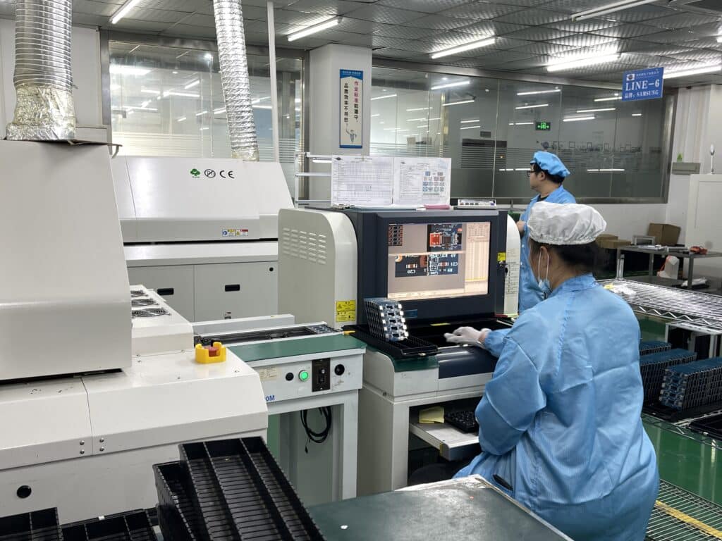
- Inspection and Quality Control: This stage involves a thorough inspection to ensure there are no defects in the assembly. This is often carried out using Automatic Optical Inspection (AOI) and X-ray inspection techniques, which we’ll delve into shortly.
- Through-Hole Component Insertion: If the board design includes through-hole components, these are inserted at this stage, either manually or automatically.
- Wave Soldering: The board then passes over a wave of molten solder, soldering the through-hole components to the board.
- Final Inspection and Functional Test: A final inspection checks that all components are functioning as they should, typically involving a power-up test to verify functionality.
4.4. Inspection and Quality Control (QC) in PCBA
QC is an integral part of the PCBA process, ensuring the assembled board is defect-free and functioning as designed. Here are some key inspection methods:
Automatic Optical Inspection (AOI): AOI uses high-definition cameras to capture images of components and solder joints on the PCBA. It checks for various defects, including misalignments, incorrect components, and inadequate soldering.
X-ray Inspection: This method is typically used for detecting hidden defects that can’t be seen on the surface, such as solder bridging and insufficient solder under BGAs (Ball Grid Arrays) and other leadless components.
Functional Testing: This is the final stage of QC, where the assembled board is powered up and tested to ensure it functions as
4.5. Types of PCBA and Assembly Methods
Just like PCBs, PCBAs also come in various types, each based on the assembly method used and the nature of the components assembled:
Surface Mount Technology (SMT) Assembly: This method uses components that are placed directly onto the surface of the PCB. These components, known as surface mount devices (SMDs), are smaller and have more connections than their through-hole counterparts, allowing for miniaturization and high-density assembly.
Through-Hole Technology (THT) Assembly: This method involves inserting the leads of components through holes drilled into the PCB and soldering them to pads on the opposite side. While this method is less common than SMT due to its lower density and manual nature, it provides stronger mechanical bonds, making it suitable for components that undergo physical stress.
Mixed Technology Assembly: This method combines SMT and THT assembly techniques, providing the benefits of both and allowing for a more flexible design.
By understanding the intricacies of PCBA, you gain a more profound appreciation for the complex processes behind everyday electronic
Let’s move onto the procurement guide:
5. Procuring PCB & PCBA: A Complete Guide
Now that you’ve gained a deeper understanding of PCB and PCBA, you might be wondering, “How do I go about procuring these for my needs?” Fear not, this section will guide you through the entire process, ensuring you’re well-equipped to make informed decisions.
5.1. Defining Your Needs
The first step to procuring PCBs or PCBAs is defining your requirements. This will largely depend on your project or product needs. For instance, you need to decide the type of PCB (such as FR-4, Aluminum, or Flexible), the number of layers, the dimensions, and the surface finish.
For PCBA, you need to consider the components that need to be assembled on the PCB, their placement, and the type of assembly technology (SMT, THT, or mixed).
5.2. Finding a Reliable Supplier
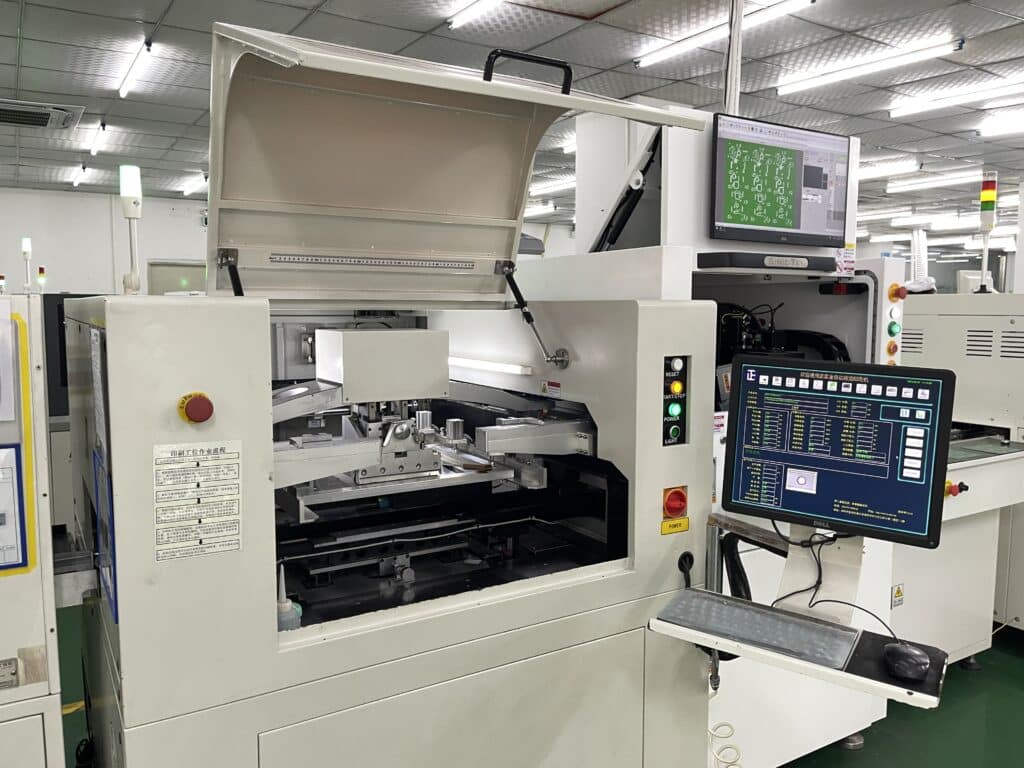
Once you’ve defined your requirements, the next step is to find a reliable supplier. Look for suppliers who have a proven track record in delivering high-quality products. Suppliers like Rowsum, with their automated production line, focus on delivering high-quality and reliable PCBs and PCBAs.
Consider the supplier’s certifications (like ISO 9001 or IPC 610), customer testimonials, and whether they offer support throughout the procurement process.
5.3. Requesting a Quote
After shortlisting potential suppliers, you should request a quote. Make sure you provide all necessary details about your requirements to get an accurate quote. Don’t forget to ask about lead times and shipping options.
5.4. Placing an Order
If you’re satisfied with the quote and the supplier’s capabilities, you can proceed to place an order. This typically involves providing the Gerber files for PCB production and the BOM (Bill of Materials) and CPL (Component Placement List) for PCBA.
5.5. Quality Control and Inspection
Once the PCBs or PCBAs are manufactured, they go through rigorous quality control checks. Make sure your supplier has a comprehensive QC process in place, which includes AOI, X-ray inspection, and functional testing. This will ensure the finished product meets your expectations.
5.6. Shipping and After-sales Support
Finally, the supplier ships the finished PCBs or PCBAs to your specified location. Reliable suppliers offer after-sales support to handle any issues or concerns that you might have post-delivery.
Remember, procuring PCBs and PCBAs is a crucial process that requires careful thought and planning. By following these steps and keeping these tips in mind, you’ll be well on your way to a successful procurement process.
I hope this guide helps you navigate your PCB and PCBA procurement journey with confidence! As always, if you have any questions, don’t hesitate to reach out. And now that you’ve got all this knowledge under your belt, are you ready to take the next step?
Get Access Now: Rowsum
6. Conclusion
In the rapidly evolving world of electronics, understanding the basics of PCB and PCBA has never been more crucial. With their wide range of applications across various industries, they form the backbone of almost all electronic devices we use daily.
We’ve traveled from the bare basics of PCBs, delving into their intricacies and jargon, moved onto the marvel of PCBA, and even walked through the procurement process. Remember, every journey with PCBs and PCBAs is unique, and yours will be too.
Knowledge and understanding are key to making the best decisions, whether you’re a procurement manager like Thomas Miller or an electronics enthusiast taking your first steps. I hope this comprehensive guide provided valuable insights and will serve as your go-to resource on your journey with PCBs and PCBAs.
Get Access Now: Rowsum
7. FAQs
1. What does PCB stand for?
PCB stands for Printed Circuit Board. It’s a board that electrically connects and mechanically supports electronic components using conductive tracks, pads, and other features etched from one or more sheet layers of copper laminated onto a non-conductive substrate.
2. What is PCBA, and how does it differ from PCB?
PCBA stands for Printed Circuit Board Assembly. While a PCB is the board itself, PCBA is the process of mounting various electronic components onto the PCB.
3. What are some of the common types of PCBs?
The common types of PCBs include Single-sided PCB, Double-sided PCB, Multilayer PCB, Rigid PCB (FR-4), Flexible PCB (FPC), and Aluminum-backed PCBs.
4. How is quality control ensured in PCBA?
Quality control in PCBA is ensured through rigorous inspection methods such as Automatic Optical Inspection (AOI), X-ray inspection, and functional testing.
5. How can I procure PCBs and PCBAs?
Procuring PCBs and PCBAs involves defining your requirements, finding a reliable supplier, requesting a quote, placing an order, and finally, shipping and after-sales support. Reputable suppliers offer support throughout this process to ensure you get the best possible product.