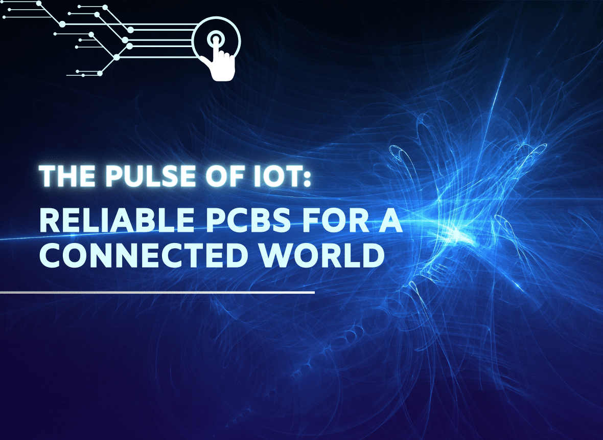
Unveiling IoT: The Nexus of Connectivity and Innovation
In the ever-evolving landscape of technology, how does the Internet of Things (IoT) redefine the way we interact with the world around us? Imagine a future where your coffee maker knows your schedule better than you do, where your car anticipates traffic before it happens, and your home adjusts its temperature as the weather changes — all seamlessly integrated through a symphony of interconnected devices. But what underpins this seamless integration? What enables these devices to operate so intelligently and autonomously?
The answer lies in specialized IoT PCB & PCBA. These printed circuit boards and assemblies are meticulously designed to handle the unique demands of IoT technology—managing power efficiently, processing data rapidly, and communicating reliably. These printed circuit boards and assemblies are engineered to control the operations of IoT devices, from simple data collection to complex automated responses. They are the definitive components that allow IoT devices to perform their designated functions efficiently and reliably.
Engineering the Core: IoT PCB Design Essentials
At the heart of every IoT device is a PCB (Printed Circuit Board) designed not just to fit, but to function within the demanding parameters of IoT applications. The design of these PCBs is fundamental to the device’s ability to perform its tasks reliably in the diverse environments IoT encompasses.
Why is IoT PCB Design Different?
IoT PCBs differ from conventional PCBs due to their operational environment and functionality. Key differences include:
| Feature | Description |
|---|---|
| Miniaturization | IoT devices are typically compact, necessitating smaller PCBs with higher component density. For instance, advancements in PCB design have led to a 30% increase in component density without compromising performance. |
| Robustness | Devices must withstand various conditions, from temperature fluctuations to movement and potential exposure to moisture. |
| Connectivity | PCBs must support various communication protocols like Wi-Fi, Bluetooth, and NFC. |
| Energy Efficiency | Many IoT devices are battery-operated or energy-harvesting, making power management a critical design aspect. |
| High-Speed Components | IoT PCBs must support high-speed signal integrity to process and transmit data quickly without interference. |
Designing for the Future
Designers are constantly innovating to create PCBs that are more efficient, reliable, and capable of supporting the next generation of IoT technology, utilizing:
- Advanced materials
- Innovative layout techniques
- Integration of components for increased data and connectivity demands
Challenges in IoT PCB Design
The complexity of IoT PCB design brings several challenges, which are addressed through:
- Signal Integrity: Ensuring high-speed data transmission without loss of quality.
- Thermal Management: Managing heat dissipation as devices become smaller and more powerful.
- Component Placement: Maximizing performance while minimizing interference in a limited space.
- Testing and Prototyping: Rigorous testing with multiple prototypes to ensure functionality.
Tailoring to Industry Needs
Different industries demand PCBs with specialized features, such as:
- Healthcare: Reliability, precision, and biocompatible materials.
- Automotive: Durability against vibrations and thermal cycling.
- Smart Home: User-friendly connectivity and aesthetic design.
- Industrial Automation: Robustness against chemicals and extreme temperatures.
Material Selection and Component Sourcing for IoT PCBs
Material Selection: The Foundation of PCB Functionality
Choosing the right materials is crucial in IoT PCB design, as it affects signal integrity, flexibility, and thermal management. High-frequency applications benefit from materials like Rogers, which provide excellent dielectric properties. For applications requiring flexibility, such as wearables, materials like polyimide are preferred due to their ability to endure bending and folding.
Key IoT PCB Components:
- Sensors: As the primary data collectors, sensors must be selected for their precision and compatibility with the IoT environment. Common types include temperature, humidity, and pressure sensors, each chosen for their specific range and sensitivity.
- Wireless Connectivity Modules: Critical for data transmission, these modules must support the necessary communication protocols like Wi-Fi, Zigbee, LoRa, Bluetooth, and NFC, chosen based on the range, data rate, and power consumption needs of the application.
- Power Management Systems: These systems are essential for managing power distribution and consumption, especially in battery-operated devices. The use of low quiescent current voltage regulators can significantly enhance battery life.
- Microcontrollers: The selection of microcontrollers is a balance between processing power and energy consumption, ensuring efficient data handling without draining power resources.
- Memory Components: Flash memory is commonly utilized for its reliability and non-volatility, essential for data logging and firmware.
Design Considerations for IoT PCBs:
- Sensor Selection: It’s imperative to match sensors to their intended application, considering factors like environmental conditions and required measurement accuracy.
- Wireless Protocol Considerations: The choice of wireless technology is dictated by the specific needs of the IoT device, including considerations for range, bandwidth, and energy efficiency.
- Power Optimization: Strategies for power management are vital, particularly for devices where longevity and battery life are critical.
Cost-Optimization in IoT PCB Production
Cost-optimization in IoT PCB production is essential for maintaining a competitive edge. Here are some strategic approaches to consider:
Design for Manufacturability (DFM):
- Component Placement: Optimize component placement for automated assembly to minimize labor costs.
- Panelization: Use standard panel sizes to maximize the number of boards per production run, improving material utilization.
- Standardization: Standardize on common component footprints to simplify assembly and reduce inventory complexity.
- Layer Reduction: Minimize the number of layers in the PCB design to decrease material usage and processing time.
Leveraging local component sourcing, especially from Chinese suppliers, can significantly reduce expenses without compromising quality. Bulk purchasing and fostering strong supplier relationships can unlock economies of scale, while investing in automated production lines and energy-efficient machinery can enhance production efficiency and sustainability.
In this context, Rowsum stands as a partner that can facilitate these cost-optimization strategies. With our expertise in DFM and established networks in component sourcing, we offer the leverage needed to reduce costs and maintain high-quality standards in IoT PCB production.
Applying PCB Principles: Interactive Transit Hub Case Study
Imagine we’re at a busy public transit hub. The interactive system here is key—it shows live updates and helps people find their way. It’s got to work all the time, no matter if it’s hot or cold outside.
So, what does it take to build such a system? It’s not just about showing maps and times. It needs to handle lots of data and stay tough against the weather. Think about the kind of tech that can do all this.
We’d pick hardware that can crunch numbers fast for routing, store tons of data safely, and keep running without eating up too much power. We’d also ensure it has robust connectivity options—perhaps integrating 5G capabilities for real-time communication and IoT functionalities to interact with other smart city systems. These aren’t random choices; they’re about making sure the system does its job well in the real world.
And tech keeps moving, right? We might want to add new stuff later, like features to help people who can’t see well. So we have to think ahead. What can we do now to make adding those features easy later on? It’s about planning for adaptability and future enhancements. It’s pretty cool to think about—not just fixing today’s problems but also getting ready for what’s next.
Remember, this scenario isn’t just a story. It’s a practical illustration of the principles we’ve discussed throughout this chapter. By considering the hardware and features of an interactive public transit system, we’re applying the concepts of PCB and PCBA design, material selection, and component sourcing in a real-world context. It’s about connecting the dots between theory and practice, ensuring that as technology evolves, our approach to design and manufacturing does too.
Conclusion
In the intricate dance of innovation, IoT PCBs and PCBAs are the pivotal steps that ensure every move is precise and every connection is seamless. Rowsum stands at the forefront, orchestrating these complex components into harmonious systems that power the future’s technology.
To explore how our expertise can elevate your technological solutions, we invite you to connect with us. For inquiries and collaborations that align with your vision of quality and efficiency, contact us at [email protected].