

Introduction
What exactly is PCB routing, and why is it crucial in the world of electronic design? This question often surfaces among professionals and enthusiasts alike who delve into the realm of PCB and IC fabrication. PCB routing is the process of connecting various components on a Printed Circuit Board (PCB) or within Integrated Circuits (ICs). It’s a critical step that follows component placement, where the accurate positioning of each component is determined. The effectiveness of PCB routing directly impacts the performance, reliability, and manufacturability of electronic devices. In this article, we explore the intricacies of PCB routing and provide practical insights to optimize your PCB design.
PCB Routing Techniques and Tips
- Trace Length Considerations
One of the fundamental aspects of PCB routing is the consideration of trace length. It’s essential to include the length of vias and the lengths of package pads in your calculations. This comprehensive approach to measuring trace length is crucial because it affects the signal integrity and timing of the circuit. Inaccurate trace length measurements can lead to signal delays and reflections, impacting the overall performance of the PCB. Therefore, precision in accounting for every part of the trace, including the vias and pads, is vital for optimal PCB design.
- Optimal Trace Angling
The angling of traces in PCB design is another critical factor. Opting for a 135-degree angle when routing traces is preferred over arbitrary angles, as improper angling can lead to manufacturing complications. The right angles help in reducing signal reflection and impedance changes, ensuring better signal integrity and reducing the potential for etching problems during fabrication. It’s a seemingly small detail that can have significant implications for the quality and manufacturability of the PCB.
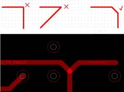
- Avoiding Sharp Angles in Trace Routing
When designing PCB traces, it is crucial to avoid right angles or acute angles. Sharp corners can lead to unwanted changes in trace width and impedance, which may cause signal reflection and, consequently, signal integrity issues. These reflections can result in crosstalk and electromagnetic interference, potentially disrupting the circuit’s performance. As depicted below, the recommended practice is to use curved traces or 45-degree angles to ensure a smoother transition for signals, which helps maintain consistent impedance and reduce the risk of signal degradation.
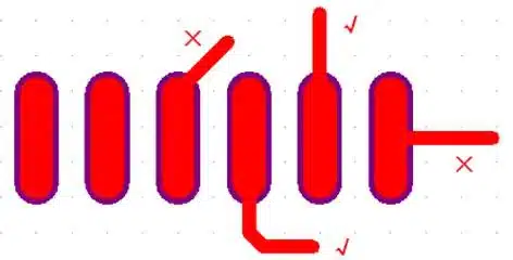
- Proper Trace Routing from Pads
When routing traces from the pads of components, it’s important to start from the lengthwise side of the pad rather than the widthwise side or the corners. Traces should ideally exit the pads in a way that avoids sharp changes in direction, with a recommended clearance of at least 6 mils from the pad edge to the trace’s corner. This practice helps in minimizing stress on the solder joints and reduces the risk of etching issues during manufacturing. The right approach to routing from pads not only facilitates a better assembly process but also contributes to the longevity and reliability of the PCB.
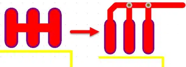
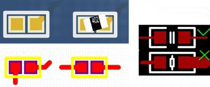
- Connection Strategy for Adjacent Soldering Pads
For adjacent pads that belong to the same network, a direct connection should be avoided. Instead, the traces should extend out from the pads before connecting. This approach prevents the formation of solder bridges during manual soldering, which could lead to short circuits. By extending the traces first, there is more space to work with, reducing the risk of soldering errors and ensuring a cleaner, more reliable connection.
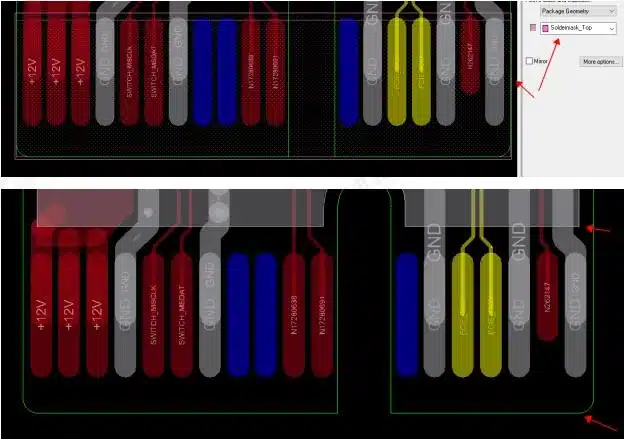
- Symmetrical Routing for Small Chip Components
Symmetry in trace routing is particularly important when dealing with small chip components. It is crucial to ensure that the traces at both ends of a component maintain consistent width. If one pin is connected with a copper pour, the opposite pin should have a similar layout. This balanced routing helps in preventing the component from shifting or rotating during the soldering process, which is vital for maintaining the integrity of the PCB assembly.
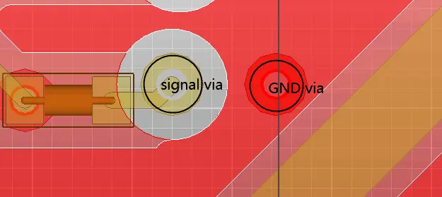
- Grounding and Placement of GND Vias
For signals that require grounding, maintaining the integrity of the ground plane is imperative. It is recommended to place GND (ground) vias strategically along the ground lines. The distance between two GND vias should not be too large; ideally, it should be within the range of 50-150 mils. Proper placement of GND vias ensures a strong and continuous ground plane, which is crucial for signal integrity and minimizing electromagnetic interference. The image below illustrates the preferred grounding practices for signals requiring a ground reference.
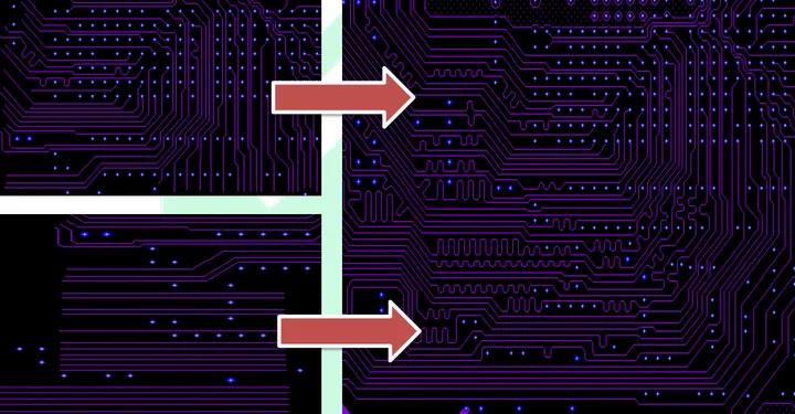
- Ensuring a Continuous Reference Layer for High-Speed Signal Routing
High-speed signal traces require a continuous and uninterrupted reference plane to maintain signal integrity. It is crucial to avoid signal routing across different zones where the reference plane may be interrupted. For high-speed signals, it is recommended that the trace maintains a minimum distance of 40 mils from the edge of the reference plane. This helps prevent issues such as impedance discontinuities and signal reflections that can degrade the performance of the circuit. The accompanying image demonstrates the ideal routing practices for high-speed signals, ensuring they remain within a continuous reference plane for optimal performance.

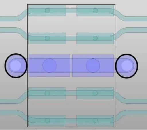
- Impedance Control for Surface-Mount Device (SMD) Pads
Surface-mounted device (SMD) pads can cause a reduction in impedance, which may lead to impedance discontinuities affecting signal integrity. To mitigate this issue, it’s advisable to remove a layer of the reference plane directly beneath the SMD pads, matching the size of the pads. This technique helps to minimize the abrupt change in impedance. Common SMD components that benefit from this practice include capacitors, ESD suppressors, common mode chokes, and connectors. The image below illustrates the recommended modification to the reference plane under SMD pads for better impedance control.
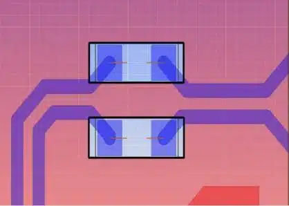
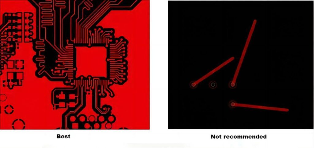
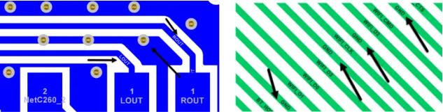
- Minimizing Loop Area in Signal Routing
In PCB design, it’s critical to minimize the loop area formed by signal traces and their return paths. A smaller loop area reduces the electromagnetic radiation emitted from the trace and also decreases the circuit’s susceptibility to external interference. As shown in the image below, the correct routing method involves making the signal path as direct as possible, thus minimizing the loop area. This practice not only improves signal integrity but also enhances the overall electromagnetic compatibility (EMC) of the PCB.
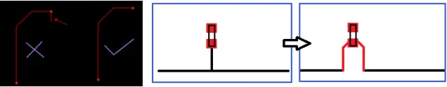
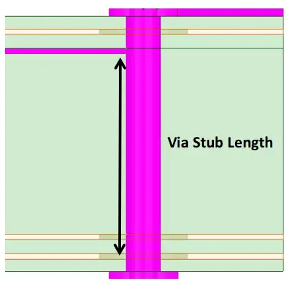
- Minimizing Stubs in PCB Routing
When routing PCBs, it is imperative to avoid the creation of stubs. A stub, which is an unconnected segment of a trace, can act as an unwanted antenna, introducing signal reflections and degradation. It is best to design traces such that the stub length is effectively zero. Additionally, the effect of via stubs—remnants of a trace left in a via after a signal switches layers—must be considered, especially when the stub length exceeds 12 mils. In such cases, it’s advisable to evaluate the impact of via stubs on signal integrity through simulation. Techniques like back-drilling can be used to remove excess via stub material and preserve signal integrity. The images below provide a visual guide on how to avoid stubs in PCB design, both in traces and vias.
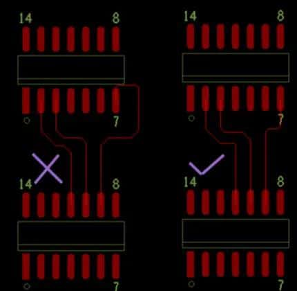
- Avoiding Loop Formation Across Different Layers
In multilayer PCB designs, it’s crucial to avoid creating loops with traces across different layers. Such loops can act as antennas, potentially causing radiative interference that can disrupt the functionality of the circuit. Ensuring that traces are routed to prevent loop formation is a key design consideration, especially when dealing with high-frequency signals where the potential for interference is greater. The image below demonstrates how to route traces properly to avoid the formation of loops and minimize the risk of radiative interference.

- Placement of Test Points on High-Speed Signals
For high-speed signal traces, it is generally recommended to refrain from placing test points. Test points can introduce discontinuities and impedance mismatches, which may lead to signal integrity issues such as reflections and attenuation. In high-speed applications, even small discontinuities can significantly disrupt signal transmission, so maintaining a smooth and consistent trace without test points is crucial for preserving the quality of the signal.
- Shielding for Interference-Prone or Sensitive Signals
Signals that are prone to interference or are particularly sensitive, such as radio-frequency (RF) signals, require careful planning for shielding. Implementing a shield, typically with a width of at least 40 mils (though maintaining a minimum of 30 mils is advisable and can be confirmed with the manufacturer), can significantly reduce interference. Additionally, placing numerous ground vias on the shield can enhance its effectiveness by ensuring a solid connection to the ground plane and improving the soldering quality.
- Uniform Trace Width Within the Same Network
Maintaining a uniform trace width within the same network is critical for consistent characteristic impedance. Variations in trace width can cause uneven impedance, leading to signal reflections, particularly at higher transmission speeds. While certain conditions, such as the lead-outs of connectors or Ball Grid Array (BGA) packages, may necessitate changes in trace width due to limited space, it is important to minimize the length of any section where the trace width is not consistent. This helps to reduce the impact on signal integrity.

- Trace Widths for IC Pinouts
For traces leading out from Integrated Circuit (IC) pins, the trace width should be less than or equal to the width of the pad. It’s crucial to avoid having the trace width be greater than the pad width to prevent soldering issues and to ensure the integrity of the electrical connection. For certain signals that require wider traces due to higher current carrying capacity, the traces can be widened approximately 6-10 mils beyond the pad to accommodate the increased current without compromising the connection. This practice ensures that the trace can handle the required current while still maintaining a robust connection to the IC pad.
- Trace Connections to Pads and Vias
It is fundamental that traces must connect to the center of pads and vias. This precision ensures reliable soldering and electrical performance. Any misalignment can lead to weak solder joints or even open circuits, which are detrimental to the PCB’s functionality. By targeting the center of pads and vias, designers can avoid these issues and maintain the integrity of the circuit connections.
- Creepage Distance for High Voltage Signals
For high voltage signals, ensuring adequate creepage distance is essential to maintain safety and prevent electrical breakdown. Creepage is the shortest path between two conductive parts, or between a conductive part and the bounding surface of the equipment, measured along the surface of the insulation. The specific creepage distance requirements vary based on voltage levels and the conditions of use, but they are critical for compliance with safety standards.
The parameters for creepage distances are as follows:
| Creepage Distance | Electrical Clearance (mm) | |
| 1. Standard AC-DC Power Supply(120VAC-240VAC) | ||
| L-N (Line to Neutral) | 3.2 mm before the fuse | 2.50 |
| 2.5 mm after the fuse | 2.00 | |
| Input-Ground | 3.40 | 2.50 |
| Rectifier Input-Output | 2.50 | 2.00 |
| Fuse In-Out | 3.20 | 2.50 |
| MOS-Ground | 4.00 | 2.80 |
| Primary-Secondary | 8.00 | 5.00 |
| Secondary-Ground | 1.40 | 0.70 |
| 2. AC-DC Power Supply with PFC Circuit | ||
| Input-Ground (PFC) | 4.50 | 2.70 |
| Primary-Secondary (PFC) | 9.00 | 5.40 |
| 3. AC-DC Power Supply Above 60V and Below 100V | ||
| Primary-Secondary (60-100V) | 3.50 | 2.00 |
| Input-Ground (60-100V) | 1.80 | 1.00 |
| V+ to V- (Pre-Fuse) | 1.80 | 1.00 |
- Routing Topology for Multiple DDR or Memory Chips
In designs that incorporate multiple DDR modules or other memory chips, it is essential to confirm the routing topology. The topology refers to the physical layout of the interconnections between the memory components, which can significantly affect performance and stability. Designers should ensure there is a reference document or a standard to follow that defines the optimal routing strategy for these components, considering factors like trace length matching and signal integrity. Having a well-planned routing topology is crucial for the correct functioning of memory interfaces, especially in high-speed applications where timing and signal quality are paramount.
- Clearance for Gold Finger Regions in Multilayer PCBs
In multilayer PCB designs, the gold finger regions—the areas of the PCB that make contact with connectors—require special attention. It is necessary to create a clearance by removing copper (known as a “window” or “slot”) beneath the gold fingers across all layers. This clearance prevents shorting and ensures that the gold fingers make reliable connections. The removed copper area should generally extend at least 3mm beyond the edge of the PCB to ensure there is no interference with the board frame or housing. Proper clearance is crucial for functionality and to prevent damage during insertion or use.
- Strategic Planning for Routing at Bottleneck Locations
When laying out a PCB, it is crucial to strategically plan for bottleneck locations within the routing channels. These are areas where the pathway narrows, potentially limiting the space available for traces. Advance planning of the channel’s narrowest sections can ensure that trace width and spacing are adequate for the signal requirements, preventing issues such as crosstalk and impedance mismatch. Proper planning helps maintain signal integrity and reduces the need for later design revisions.
- Placement of Coupling Capacitors
For optimal performance in PCB design, coupling capacitors should be placed as close as possible to the connectors they are associated with. This proximity minimizes the loop area and thus reduces electromagnetic interference (EMI). It also ensures that any noise present on the signal lines is quickly shunted to ground before it can affect other parts of the circuit. Strategic placement of coupling capacitors is a key consideration in high-speed circuit design to maintain signal integrity and minimize potential noise issues.
- Placement of Series and Termination Resistors
In PCB design, series resistors should be placed close to the transmitting device, while termination resistors are best positioned near the receiving end. For instance, series resistors on an eMMC clock signal are recommended to be located within 400 mils of the CPU. This placement ensures that the signal integrity is maintained by matching the impedance and minimizing reflections, which is critical for the high-speed signals typically found in memory and processor interfaces.
- Ground Via Placement for IC Pads
It is recommended to place at least one ground via on each ground pad of ICs, such as eMMC or FLASH memory chips. This practice effectively shortens the return path for signals, which is vital for maintaining signal integrity and reducing electromagnetic interference (EMI). Proper ground via placement can significantly improve the electrical performance of high-speed digital circuits by providing a low-impedance path to ground.

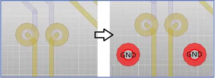
- Ground Via Placement for ESD Devices
For Electrostatic Discharge (ESD) protection devices, it is advisable to place a ground via on every ground pad. This configuration ensures that the ESD current can be quickly and efficiently routed to the ground plane, enhancing the protective effect. The ground vias should be placed as close as possible to the pads to minimize the inductance and resistance of the path to ground. The image below depicts the recommended placement of ground vias for ESD devices to maximize their effectiveness.
- Routing Considerations Around Sensitive Components
In PCB layout, it is crucial to avoid routing traces around sensitive components such as crystals, oscillators, clock generators, clock distributors, switch-mode power supplies, magnetic devices, and connector through-holes. These components are often susceptible to noise and can be sources of interference themselves. Traces routed too close to these components can introduce unwanted noise or be affected by the interference, leading to potential issues with signal integrity and circuit performance. Therefore, maintaining a clear area around these components is essential for ensuring the stability and reliability of the PCB.
- Layer Transition and Via Management for Signal Integrity
In PCB design, when a signal trace changes layers and both layers are referenced to the ground plane, it’s important to place an accompanying ground via adjacent to the signal via. This ensures continuity of the return path and maintains signal integrity. For differential signals, both the signal via and the accompanying ground via should be symmetrically placed to preserve the differential pair’s impedance and minimize crosstalk. In the case of single-ended signals, placing a return ground via next to the signal via reduces the inter-via crosstalk and supports signal integrity.
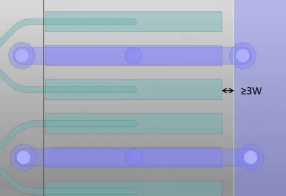
- Ground Copper Clearance for Connectors
When designing PCB connectors, it is crucial to ensure that the ground copper extends a distance of at least three times the trace width away from the signal pads. This spacing, denoted as ≥3W in technical terms, helps to prevent crosstalk and electromagnetic interference (EMI) between the ground and signal lines, which is vital for maintaining signal integrity. The illustration below demonstrates the recommended ground copper clearance for connectors, a key design parameter for robust PCB layout.
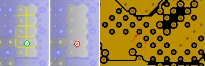
- Maintaining Plane Integrity in BGA Regions
For areas under Ball Grid Array (BGA) packages, it’s important to maintain the integrity of the plane layers. If there is a break in the plane, it should be bridged with traces or the board should be modified through a process called “thinning” or “sculpting” to ensure continuity. This practice avoids compromising the power or ground planes’ effectiveness, which can lead to issues with power distribution and signal integrity. The image below illustrates the correct method to bridge any gaps in the plane under BGA regions, which is essential for the proper functioning of the PCB.
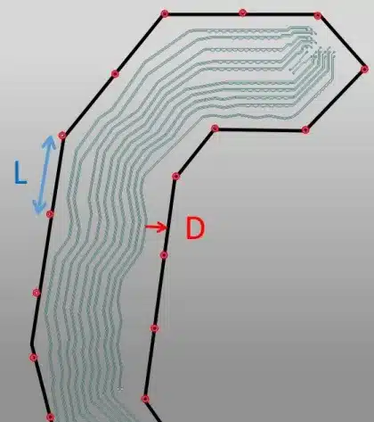
- Ground Shielding in PCB Routing
When PCB routing involves ground shielding, it is recommended to follow the practices as depicted in the image. L represents the spacing between ground vias in the shielding, and D indicates the distance between the ground shield and signal traces. For effective shielding, the distance D should be at least four times the trace width (≥4*W). This ensures minimal interference from the ground shield to the signal lines, maintaining signal integrity throughout the PCB.
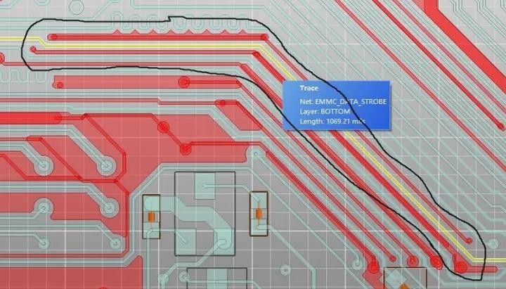
- Ground Shielding for High-Speed Single-Ended Signals
Certain critical high-speed single-ended signals, such as clock signals, reset lines (e.g., emmc_clk, emmc_datastrobe, RGMII_CLK), should be shielded with a ground trace. It is advisable to place a ground via at least every 500 mils along the ground shield to ensure an effective low-impedance path to ground. This practice helps in minimizing noise and preserving signal integrity for these sensitive high-speed signals. The image below showcases the recommended placement of ground vias along the ground shield for such signals.
Conclusion
Our journey through the essentials of PCB design has been enriched by the insights provided by Huowa from Zhihu. With Huowa’s permission, we’ve adapted his expert advice to fit our narrative, aiming to share a clear and actionable guide with you.