Ever pondered why certain electronic devices seem to function better than others, or why some gadgets last notably longer? The answer might be closer than you think, right on the surface of their printed circuit boards (PCBs). In the competitive world of electronics manufacturing, the choices made at the microscopic level can have macroscopic impacts. The decision often hinges on the type of surface treatment used on the PCB. specifically PCB ENIG, a finish that consistently stands out.
Why is ENIG so special? ENIG stands for Electroless Nickel Immersion Gold, a premier finishing method for PCBs. It offers enhanced conductivity, exceptional resistance to oxidation, and promotes device longevity. For professionals in the electronics industry who prioritize both durability and efficiency, PCBs with an ENIG finish are frequently favored.
What is PCB ENIG?
Diving Deep into Electroless Nickel Immersion Gold:
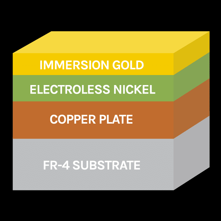
Electroless Nickel Immersion Gold, known as ENIG, is a distinct surface finishing approach for PCB. Comprising two distinct layers, ENIG plays a pivotal role in enhancing the performance and longevity of electronic devices.
- Nickel-Phosphorus Alloy Layer: This foundational layer, predominantly a mix of nickel and phosphorus, adheres directly to the PCB’s copper surface. Its main function is to serve as a protective shield, stopping the copper from rusting and providing a firm foundation for the gold layer that follows.
- Immersion Gold: While this layer might be thin, its importance can’t be overstated. It’s the protective shield for the underlying nickel.
About ENIG’s Thickness:
- Nickel Layer: This layer usually measures between 4-7 μm. It’s like the sturdy wall that guards against corrosion and sets a solid stage for the gold layer that follows.
- Gold Layer: It’s a whisper-thin layer, often between 0.05-0.23 μm. But don’t let its thinness fool you; it’s the guardian of the nickel layer and a champion of solderability.
What’s in ENIG?
- The Nickel-Phosphorus layer is primarily a blend of, well, nickel and phosphorus. Simple, but effective.
The Journey of Applying ENIG to a PCB:
- Step 1: Cleaning: First things first, we ensure the PCB surface is squeaky clean. No unwanted guests allowed!
- Step 2: Activation: We prep the copper pads on the PCB with a palladium catalyst. Think of it as a wake-up call for the copper pads.
- Step 3: Nickel Time: A chemical dance ensues, and a nickel layer gracefully covers the activated copper pads.
- Step 4: Gold’s Grand Entrance: The PCB takes a gold bath, and a fine layer of gold settles over the nickel.
Benefits of Using ENIG for PCB
Enhanced Conductivity
One of the primary reasons manufacturers opt for ENIG is its superior electrical conductivity. The gold layer ensures minimal signal loss, making it ideal for high-frequency applications.
Technical Detail: Gold, as a metal, boasts a conductivity nearing 45 million Siemens for every meter (S/m) when measured at ambient temperature. This high conductivity ensures minimal signal loss, making ENIG ideal for high-frequency applications.
Exceptional Resistance to Oxidation
The gold layer in ENIG acts as a barrier against environmental factors, preventing oxidation. This ensures the PCB remains functional even in challenging conditions, extending its lifespan.
Improved Solderability
ENIG-coated PCBs offer excellent solderability. The gold layer ensures a uniform and sleek surface, promoting reliable solder connections crucial for optimal device functionality.
RoHS Compliance
ENIG finishes are compliant with the Restriction of Hazardous Substances (RoHS) directive. This means that PCBs with ENIG finishes lack harmful chemicals, rendering them eco-friendly and suitable for application in various applications.
Consistent Thickness
A distinguishing characteristic of ENIG is the consistent thickness of its gold layer, which usually falls between 1-2μm. This uniformity contributes to the PCB’s stable performance.
Long-Term Reliability
With its dual-layer protection, PCB ENIG guarantees long-term reliability. The combination of nickel and gold offers protection against wear, corrosion, and environmental factors, ensuring the PCB’s longevity.
Technical Insight: The combined shield of nickel and gold provides resilience to wear, safeguards against corrosion, and withstands environmental challenges.The nickel layer often contains 4-9% phosphorus, which bolsters its resistance to corrosion.
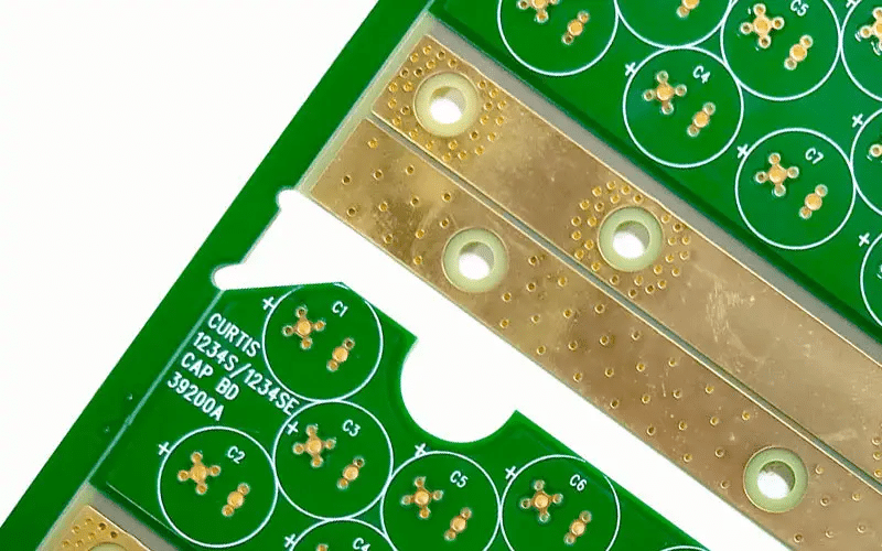
Visually Appealing Surface
Beyond its functional benefits, ENIG provides PCBs with a shiny, golden finish. This not only makes the board look premium but also aids in visual inspections, as defects are easier to spot.
Suitable for Fine Pitch Components
Given its flat surface, ENIG is ideal for PCBs with fine pitch components. This guarantees precise placement and soldering of minute components, essential in today’s electronics that lean towards compact designs.
Drawbacks :
While ENIG offers numerous advantages, it’s essential to be aware of its potential shortcomings:
Price Considerations: Typically, ENIG comes at a steeper price compared to finishes like HASL.
Difficulty in Rework: Due to the flatness and the nature of the gold layer, reworking or repairing ENIG-coated PCBs can be more challenging.
Signal Loss Over Time: Over extended periods, especially in high-frequency applications, there can be a slight degradation in signal quality.
Black Pad Phenomenon: This refers to a manufacturing challenge sometimes associated with the ENIG process.
Potential for “Black Nickel”: This occurs when the nickel layer oxidizes before the gold layer is applied, compromising the integrity of the solder joint.This issue emerges when the nickel solution has an overabundance of phosphorus, causing the nickel layer to corrode.
ENIG Compared to Alternative Surface Finishes
Choosing the right surface finish for PCBs is crucial. Each type of finish has its unique traits, pros, and potential cons. Let’s see how ENIG stacks up against other popular choices:
ENIG vs. HASL (Hot Air Solder Leveling)
- Advantages of HASL: Economical and a popular choice. Well-suited for through-hole components.
- Limitations of HASL: Can have uneven surfaces, less suitable for fine-pitch components.
- Comparison: While HASL offers a cost advantage, ENIG provides a smoother finish, making it a top pick for modern electronics that utilize fine-pitch components.
ENIG vs. OSP (Organic Solderability Preservatives)
- Advantages of OSP: Flat surface, environmentally friendly, and cost-effective.
- Drawbacks of OSP: Limited shelf life, not ideal for multiple reflow/assembly processes.
- Comparison: ENIG has an extended shelf life and adapts better to various assembly procedures, positioning it as a trusted option for intricate electronic devices.
ENIG vs. Immersion Silver
- Advantages of Immersion Silver: Flat surface, good for fine-pitch components.
- Drawbacks of Immersion Silver: Tarnishes easily, sensitive to handling and environmental conditions.
- Comparison: While both provide flat surfaces, ENIG is more robust against environmental factors and handling, ensuring longevity and reliability.
ENIG vs. Immersion Tin
- Advantages of Immersion Tin: Flat surface, lead-free.
- Drawbacks of Immersion Tin: Sensitive to handling, can whisker over time.
- Comparison: ENIG’s gold layer offers better protection against environmental factors and doesn’t whisker, making it a more stable and reliable choice.
ENIG vs. Electrolytic Nickel/Gold (Hard Gold)
- Advantages of Hard Gold: Durable, ideal for edge connectors.
- Drawbacks of Hard Gold: Expensive, not suitable for soldering due to its hardness.
- Comparison: While hard gold is more durable, ENIG offers better solderability and is more cost-effective for overall PCB coverage.
| Feature/Surface Finish Method | ENIG | HASL | OSP | Immersion Silver | Immersion Tin | Hard Gold |
|---|---|---|---|---|---|---|
| Smoothness | Excellent | Fair | Good | Good | Good | Fair |
| Oxidation Resistance | Excellent | Fair | Good | Fair | Fair | Good |
| Solderability | Excellent | Good | Fair | Good | Good | Poor |
| Cost | Higher | Lower | Medium | Medium | Medium | Highest |
| Rework Difficulty | Moderate | Easy | Easy | Easy | Easy | Hard |
| Aesthetics | Excellent | Good | Fair | Good | Fair | Excellent |
| RoHS Compliance | Yes | Depends (lead-free versions available) | Yes | Yes | Yes | Depends |
| Signal Loss Over Time | Slight (in high-frequency applications) | Moderate | Low | Low | Low | Low |
| Susceptibility to “Black Pad” | Yes | No | No | No | No | No |
Choosing ENIG for Your PCB Needs
In the vast realm of electronics manufacturing, selecting the right surface finish for PCBs can be a pivotal decision. ENIG, with its myriad of benefits, often emerges as a top contender. But when should you specifically opt for ENIG?
When is ENIG the Right Choice?
- High-Frequency Applications: Devices operating in high-frequency environments require consistent signal integrity. ENIG’s superior conductivity makes it the go-to choice in such scenarios.
- Fine Pitch Components: Modern PCB designs often include components with very close pin spacing. The smooth finish of ENIG guarantees precise soldering and connection, minimizing the chances of flaws.
- Long-Term Storage: If your production cycle involves storing unassembled PCBs for extended periods, ENIG’s resistance to oxidation ensures they remain in pristine condition, ready for assembly when needed.
- Lead-Free Requirements: With global shifts towards environmentally friendly manufacturing, adhering to RoHS standards is crucial. ENIG provides a compliant and reliable solution, ensuring your products meet international regulations.
- Cost Considerations: It’s essential to note that while ENIG offers numerous advantages, it typically comes at a higher cost compared to traditional finishes like HASL-LF.
FAQ about ENIG PCB
- What does ENIG signify in PCB context?
- ENIG, standing for Electroless Nickel Immersion Gold, denotes a specific PCB surface treatment designed to shield PCBs from corrosion and various imperfections. This technique uses a two-tiered metallic coat, with a delicate layer of gold resting on an electroless nickel base.
- Why opt for ENIG PCBs? What are its advantages?
- ENIG-coated PCBs are like the Swiss army knives of the PCB world. They’re smooth, resist oxidation, perform electrically well, can handle heat, last long, and are eco-friendly.
- What are the Disadvantages of ENIG PCBs?
- Nothing’s perfect. ENIG PCBs can be pricier, a bit tricky to fix if there’s an issue, might experience minor signal issues over a long time, and there’s this thing called the “black pad” issue to watch out for.
- Is ENIG Plating Lead-free?
- Yes, ENIG plating is lead-free and conforms to the RoHS directive, making it environmentally friendly.
- How thick is the ENIG Plating on PCBs?
- The nickel layer is usually between 4 to 7 μm thick, while the gold layer is a slender 0.05 – 0.23 μm.
- How does ENIG Plating Compare with Hard Gold Plating?
- ENIG and hard gold plating differ in several ways, including the method of gold attachment, thickness, cost, and suitability for soldering.
- What is the Shelf Life of ENIG PCB?
- ENIG PCBs can be stored for an average of 12 months, offering a longer shelf life compared to other finishes.
- How might oxidation occur on an ENIG PCB?
- If the density of gold and nickel dips beneath the necessary thresholds, they can become porous, leading to oxidation. Mishandling, like direct contact or suboptimal storage conditions, can further exacerbate this issue.
- What considerations are essential for ENIG Plating?
- When considering ENIG plating, it’s essential to be aware of the costs, potential for black pad issues, and the specific requirements of the plating process.
Conclusion
In the vast landscape of electronics manufacturing, the nuances often dictate the narrative. ENIG emerges not as a mere choice, but as a strategic decision, influencing the very core of device reliability and efficiency. It’s the silent champion behind many high-performing electronics, underscoring the adage: excellence lies in the details. As the industry evolves, those details will define the leaders from the followers, and ENIG will undoubtedly play a pivotal role in that distinction.