Introduction
Why does PCB Functional Testing matter in electronics manufacturing, and what are its key challenges? In the intricate world of electronic components, ensuring that each piece functions correctly is not just about meeting design specifications – it’s about delivering reliability and user satisfaction. PCB Functional Testing, therefore, is not a mere step in the manufacturing process; it’s a critical validation that determines whether a PCB is ready to leave the factory floor.
PCB Functional Testing is a comprehensive approach that involves a variety of tests such as Static Functional Testing (SFT), Dynamic Functional Testing (DFT), Boundary Scan Testing, and Environmental Testing. Each of these tests is designed to assess different aspects of the PCB’s performance, ensuring that the final product operates as intended, meets quality standards, and adheres to user experience expectations. This meticulous testing process is crucial for identifying manufacturing defects, incorrect or missing components, and potential operational failures, thus safeguarding product reliability and maintaining consumer trust.
Key Techniques in PCB Functional Testing
In PCB manufacturing, Functional Testing is a crucial process ensuring the highest quality and performance of electronic products. Let’s delve deeper into these sophisticated techniques:
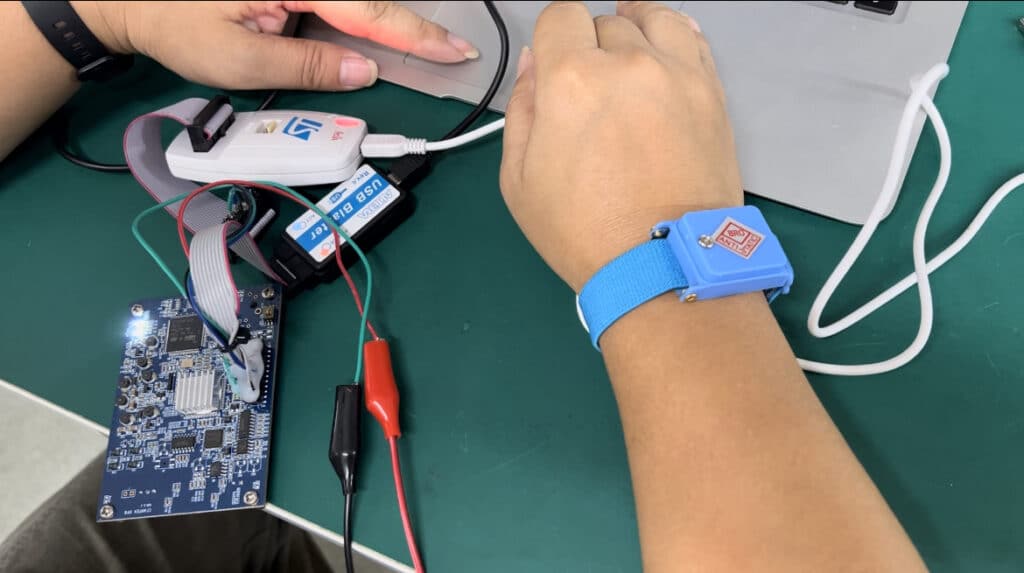
Programming Testing (Firmware Programming):
- Essential Software-Hardware Integration: After discussing the hardware-focused testing methods, introduce Programming Testing. This process involves loading and testing the firmware or software on the PCBs to ensure that it functions correctly with the hardware.
- Real-World Operation Simulation: Explain how this test is critical for verifying that the PCB operates as intended in its final use. It simulates the real operational environment, ensuring that both the hardware and embedded software perform seamlessly together.
- Tools and Process: Describe the specialized equipment and software used for this testing, such as in-system programming (ISP) tools, firmware loading stations, and debugging tools. Discuss the process of programming the PCB, verifying the software integration, and testing for operational functionality.
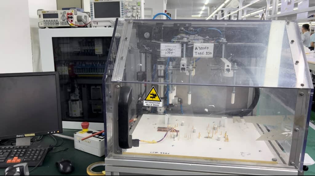
Static Functional Testing (SFT):
- The Precision Check: SFT meticulously examines each static component of a PCB, akin to a surgeon’s detailed inspection. Technicians use precision tools like digital multimeters to measure resistances and capacitances, ensuring that each component is not just close but precisely aligned with the design specifications.
- Detecting Subtle Flaws: This method is particularly effective in identifying marginal discrepancies in resistors or capacitors. Small errors, often undetectable in other testing stages, are caught here, preventing potential major malfunctions down the line.
Dynamic Functional Testing (DFT):
- Bringing PCBs to Life: DFT awakens the PCB from its static state. By applying power and simulating operational conditions, DFT examines the PCB’s dynamic responses. Tools such as signal generators and oscilloscopes are employed to test the board’s performance, mimicking a real-life operational environment.
- Assessing Under Stress: DFT evaluates how the PCB performs under various operational stresses, including fluctuating frequencies and power conditions. This phase is crucial for ensuring the PCB can handle its intended operational load without failing.
Boundary Scan Testing:
- The Non-Invasive Detective: Utilizing the JTAG standard, Boundary Scan provides a non-intrusive method to examine the PCB’s internal digital circuits. This technique is essential for complex PCBs where physical probing is not feasible. It involves scanning the integrity of connections and pathways within integrated circuits, uncovering issues like shorts or open circuits.
- A Comprehensive Scan: Specialized software is used for Boundary Scan, allowing for a thorough and detailed examination of the PCB’s digital components.
Environmental Testing:
- The Ultimate Endurance Test: PCBs are subjected to extreme environmental conditions in this test. It involves placing the PCB in environmental chambers that simulate varying temperatures, humidity levels, and vibrations to assess the board’s durability and performance under harsh conditions.
- Simulating Harsh Realities: Critical for PCBs intended for use in demanding environments, this test ensures the PCB’s longevity and reliability, no matter the external conditions it may face.
The Benefits of Effective PCB Functional Testing
PCB Functional Testing stands as a critical pillar in the electronics manufacturing industry, not just assuring quality but crafting excellence. Here’s a deeper dive into its multifaceted benefits:
1. Elevating Reliability and Minimizing Failure Risks:
- Proactive Error Prevention: Beyond detecting faults, Functional Testing strategically prevents them. By employing advanced algorithms and precise measurement tools, it ensures that each PCB component operates flawlessly, significantly reducing the likelihood of future failures.
- Quantitative Analysis for Quality: Employing statistical methods, Functional Testing quantifies the reliability of PCBs, offering empirical evidence of their superior performance. This data-driven approach is essential for manufacturers committed to upholding the highest standards of quality.
2. Meticulous Evaluation for Optimal Functionality:
- Holistic Component Analysis: This testing method evaluates the interaction between various PCB elements, much like verifying the precise workings of a complex clock mechanism. Each gear and cog must align perfectly to ensure accurate timekeeping, mirroring how every component on a PCB must function in sync for optimal performance.
- Realistic Stress Testing: Simulating real-world conditions, Functional Testing rigorously assesses PCB performance under varying electrical loads and environmental stressors. This includes thermal cycling and vibration testing, crucial for products used in dynamic or extreme environments.
3. System-Wide Insights for Enhanced Performance:
- Integration Efficiency Analysis: Functional Testing not only scrutinizes the PCB but also examines its synergy with connected modules. This includes evaluating signal integrity and electromagnetic compatibility, ensuring seamless integration within larger systems.
- Advancing Hardware-Software Integration: In our increasingly digital world, ensuring that PCBs effectively communicate with their software counterparts is paramount. This testing phase involves complex protocols to evaluate software interactions, critical for IoT and smart devices.
- Sustainability Through Power Optimization: A significant aspect of Functional Testing is assessing power consumption patterns. By optimizing power usage, it contributes to the sustainability of the final product, a growing concern in modern electronics design.
- User-Centric Design Validation: Functional Testing plays a pivotal role in confirming that the PCB design translates into a user-friendly experience. This includes testing user interface components and ensuring reliability in user-centric operations.
- Compliance and Safety Assurance: Adhering to global standards like RoHS, WEEE, and IPC, Functional Testing verifies that PCBs meet all necessary safety and environmental regulations, an indispensable aspect for global market access.
Diverse Methods in PCB Functional Testing
The field of PCB manufacturing employs a variety of functional testing methods, each serving specific purposes. Here’s a concise overview of some of the most common techniques:
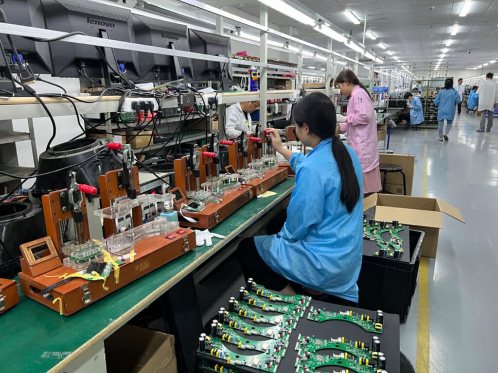
In-Circuit Testing (ICT):
- ICT involves checking the PCB for shorts, opens, resistance, and capacitance issues. It’s a thorough method typically used for mass-produced PCBs to ensure high reliability.
Automated Optical Inspection (AOI):
- AOI uses visual inspection systems to detect surface-level defects such as soldering errors and component misalignments. It’s crucial for verifying the accuracy of PCB assembly.
Flying Probe Test:
- This method uses movable probes to test the electrical performance of PCBs. Ideal for low-volume or prototype PCBs, it offers flexibility without the need for custom fixtures.
X-Ray Inspection:
- X-Ray inspection allows for non-destructive examination of internal PCB structures, including layer alignment and hidden solder joints. It’s vital for complex multi-layer PCBs.
Burn-In Testing:
- Burn-In Testing subjects PCBs to prolonged operation under extreme conditions to identify potential early-life failures. It’s a stress test that ensures long-term reliability.
The Practical Process of Conducting PCB Functional Testing
Preparing for Programming Testing:
- Essential Preparations: Clients should provide detailed firmware programs, the specific methods for programming, and comprehensive testing procedures to ensure an efficient testing process.
- Maintaining Confidentiality: Emphasize the importance of protecting proprietary information. Discuss the measures taken by the manufacturer to ensure the security and confidentiality of client-provided software and data.
Complexity and Efficiency Considerations:
- Streamlining the Process: Advise clients on the need to consider the simplicity of the programming and testing process, crucial for scaling up in mass production while minimizing labor and time costs.
- Evaluating Scalability: Highlight how choosing scalable testing methods can impact the efficiency and cost-effectiveness of large-scale production runs.
Cost and Timeline Management:
- Budgeting for Testing: Provide guidance on budgeting for Programming Testing, including potential additional costs.
- Production Timeline Impacts: Discuss how incorporating Programming Testing may influence the overall production timeline and strategies to minimize delays.
Technical Requirements and Specifications:
- Clear Specifications Needed: Clients should prepare detailed technical specifications for their firmware, aiding the manufacturer in conducting precise and effective tests.
- Importance of Version Control: Stress the importance of using the most current and stable firmware version, ensuring the effectiveness of the testing process.
Collaborative Feedback and Iteration:
- Effective Communication: Outline the process for providing clients with feedback on testing results and any necessary firmware revisions.
- Joint Effort in Refinement: Emphasize the collaborative nature of refining firmware based on testing outcomes, fostering a partnership approach.
Post-Testing Support and Documentation:
- Continued Assistance: Explain the manufacturer’s commitment to post-testing support, addressing any issues that arise during testing.
- Comprehensive Documentation: Highlight the importance of providing clients with detailed documentation of the testing process and results for their records.
Ensuring Compliance and Certification:
- Meeting Industry Standards: Discuss how Programming Testing contributes to meeting regulatory compliance and industry certifications, a critical aspect for many clients.
Conclusion
PCB Functional Testing is about precision, reliability, and ensuring your electronics meet the highest standards. We’ve covered everything from the thoroughness of Static and Dynamic Testing to the critical role of Programming Testing. It’s about making sure your PCBs aren’t just made, but made right.
If you’re looking for expertise in PCB Functional Testing, Rowsum is here to deliver. We focus on detail, quality, and customer satisfaction to bring your projects to their full potential.